![]()
Cisco Nexus SmartNIC+ V9P
The Cisco Nexus SmartNIC+ V9P (formerly ExaNIC V9P) is an FPGA based network application card, specifically optimized for low-latency and high density datacenter applications. The device is built around a powerful Virtex Ultrascale Plus (VU9P) FPGA, packaged into a compact, half-height half-length, form factor, featuring dual QSFP-DD interfaces (8 lanes each) and 9GB of DDR4 DRAM.
Device installation
Installation of the SmartNIC+ V9P is similar to other Cisco Nexus SmartNIC devices. This page should be used in conjunction with the SmartNIC Installation section.
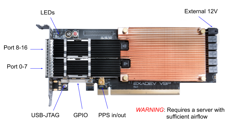
Cooling
The SmartNIC+ V9P is available only in a passively cooled variant. This means that suitable airflow must be provided by the enclosing server. As an example, Dell R630 and R640 servers are suitable for this use case. It is expected that any similar server platform will be sufficient.
Firmware recovery
The firmware recovery procedure for the SmartNIC+ V9P differs from other SmartNIC devices and requires JTAG access to the device. To recover an SmartNIC+ V9P:
- From a cold boot of the host, hold the SmartNIC+ V9P recovery button and power up the host.
- After booting, open Vivado and connect to the SmartNIC+ V9P via JTAG. It will appear in Vivado as an
xcvu9pdevice. - This device should then be programmed with a known-good bitfile that has been built with
NOREBOOT=1. A bitfile of thenative_nic_examplewhich can be used for this purpose is available via Cisco TAC. - Reboot the server.
The SmartNIC+ V9P should now be recovered with regular NIC functionality.
JTAG Access
The SmartNIC+ V9P features an onboard USB to JTAG adapter. Users can plug the supplied USB cable into the 4 pin USB header (J5). It will appear as a supported JTAG device in Xilinx Vivado.
GPIO
A small header (J4) is on the SmartNIC+ V9P that exposes 4 bits of user GPIO. Please create a case with Cisco TAC for further details on this interface.
PPS
An MCX connector is onboard for PPS in/out time synchronization. Due to size & area restrictions, this connector could not be placed on the PCIe bracket. To use the connector, it is suggested that users run a small loom from the MCX connector to just outside the bracket for connection to a PPS network.
FPGA Firmware Development
A Firmware Development Kit is available for the SmartNIC+ V9P to simplify FPGA development, which includes Cisco's low latency PCS/MAC and DMA engine. Further details on the FDK can be found on our FDK Documentation Site.
For customers using their own IP, the following hardware specific notes may be helpful:
- The full Xilinx part number is XCVU9P-L2FLGA2104E
- A "-L2" speed grade is loaded by default. This part is normally operated at -2 speed grade, but can be run at a lower core voltage (0.72V instead of 0.85V) with "-1" speed grade builds to reduce thermal dissipation. Please contact Exablaze for further details.
- The configuration memory attached is a Micron MT28EW01GABA1LPC-0SIT (NOR BPI x16)
- The PCIe reset net
PERSTN0is inverted on the PCB. When using the Xilinx PCIe core, the System Reset Polarity dropdown will need to be set to ACTIVE HIGH. - PCIe lanes are connected to banks 225-227, with PCIe REFCLK connected to MGTREFCLK0_225, pins AL9/AL8
- PCIe lane reversal is in use (FYI only, the PCIe core will detect and deal with this)
-
161M reference clocks are supplied to the following locations:
- Bank 126 MGTREFCLK0_128, pins V38/V39
- Bank 232 MGTREFCLK0_232, pins R9/R8
- Bank 43, pins AJ32/AK32
-
The following GTY transceiver channels have their polarity inverted on the PCB - the transceiver IP core will need to have
rx_pol/tx_polset for these:- Bank 126, RX channel 2, pins R45/R46
- Bank 126, RX channel 3, pins N45/N46
- Bank 126, TX channel 2, pins M42/M43
- Bank 126, TX channel 3, pins K42/K43
- Bank 127, RX channel 0, pins L45/L46
- Bank 127, RX channel 1, pins J45/J46
- Bank 127, RX channel 3, pins E45/E46
- Bank 127, TX channel 0, pins H42/H43
- Bank 127, TX channel 1, pins F42/F43
- Bank 127, TX channel 3, pins B42/B43
- Bank 232, RX channel 0, pins T2/T1
- Bank 232, RX channel 2, pins P2/P1
- Bank 232, TX channel 0, pins L5/L4
- Bank 232, TX channel 2, pins J5/J4
- Bank 233, RX channel 0, pins K2/K1
- Bank 233, RX channel 3, pins D2/D1
- Bank 233, TX channel 0, pins G5/G4
- Bank 233, TX channel 0, pins C5/C4
This page was last updated on Apr-06-2021.