Overview
The Cisco Nexus SmartNIC (formerly ExaNIC) FPGA development kit unlocks the FPGA technology within the SmartNIC, allowing customers to develop applications that run directly within the network card firmware. This allows for a number of interesting applications, some of which are demonstrated in examples provided with the development kit. The following examples (referred to as targets) come with the development kit, including the requisite source code for each:
- A 'native nic example' which implements a NIC by connecting the PCS modules of all the ports to the host.
- A 'trigger example' shows how to pre-load the card with a reply ahead of time, and send it based on a simple mask/pattern match over received frames.
- A 'ping example' demonstrates various functionality, including sending frames directly from the card, making use of hardware timestamping, and using custom frames to communicate with software.
- A 'steering example' demonstrates how to perform user-defined flow steering. A simple destination IP based flow steering example is provided, which can easily be modified to perform steering based on application layer information.
- A 'bridging example' demonstrates how to bridge two ports together, such that traffic received on one port is transmitted out of another.
- A 'soft responder exampler' assists with one method of benchmarking the MAC latency of the SmartNIC. This example simply sends a response packet on receipt of the first byte off the wire.
- A 'native loopback example' forwards received packets out a different port, including clock domain crossing from RX to TX and buffering.
- A 'chipscope example' allows users to easily see relevant signals in chipscope, making performance measurement and debugging easy.
- A 'multi preload tx example' allows the user to preload frames into the memory of the FPGA and then send them out several ports simultaneously in response to a single register write.
- A 'native register example' which is a minimal example of how to use the PCI register interface.
- A 'native spam example' which implements a simple packet generator.
- An 'extra BARs example' which demonstrates how to use the additional register/memory spaces at BAR1/BAR4.
- A 'nic 256b host if example' which implements a NIC by connecting the PCS modules of all the ports to the host using the 256 bit rx host interface.
- A 'host spam example' which generates and sends packets to the host from the FPGA.
A mailing list is available to be notified when updates to the SmartNIC FDK are released. Please feel free to add yourself here.
Installation
A Linux environment is recommended for installing the FDK, as the build scripts are currently intended for a Linux environment.
Prior to using the development kit customers must install Xilinx Vivado, which can be obtained from the Xilinx website. Vivado 2018.3 or later is recommended.
The following models are supported by the free WebPACK edition of Vivado.
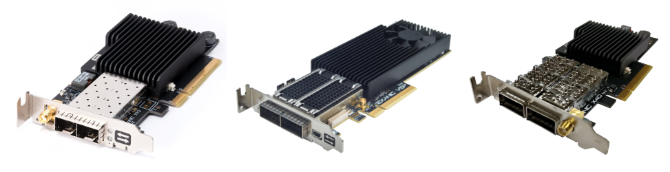
- Cisco Nexus SmartNIC K35-S (formerly X10) (XCKU035 FPGA)
- Cisco Nexus SmartNIC K35-Q (formerly X40) (XCKU035 FPGA)
- Cisco Nexus SmartNIC K3P-S (formerly X25) (XCKU3P FPGA)
- Cisco Nexus SmartNIC K3P-Q (formerly X100) (XCKU3P FPGA)
A paid Vivado license is not required to use the FDK on these cards.
The larger XCVU5P and XCVU9P FPGAs on the Cisco Nexus SmartNIC+ V5P and Cisco Nexus SmartNIC+ V9P are not supported by the WebPACK edition of Vivado and will require an evaluation or full Vivado license.
The SmartNIC development kit ships as a tar file that contains a project directory structure. Untar the project directory structure to a convenient location.
Licensing
The FDK is available in three main variants:
- "full": Full licensed version
- "eval": Time limited demonstration version that can be used to evaluate the full version on a test system. After two hours of operation, portions of the SmartNIC will start to shut down and can only be reset by rebooting the host.
- "free" (new from version 2.7.0): Free to use (and not time limited) but has extra latency of around 35ns in PCS and PCIE in both RX and TX directions. Not recommended for ultra low latency applications.
To inquire about purchasing the full version, contact your reseller or our sales team.
License installation
Cisco provides a license file which Xilinx Vivado will require in order to synthesize the "full" version of the development kit. Note that this is not required or provided for "eval" or "free" FDKs.
The license file can be installed either locally or on a license server.
For local installation, the license file can be placed in your ~/.Xilinx/ directory. You may also need to update your ~/.flexlmrc file to ensure that it has the ~/.Xilinx/ directory in the license search path, it should contain a line similar to:
XILINXD_LICENSE_FILE=/home/username/.Xilinx
For installation on a license server, first edit the first line of the license file to contain the correct server name in place of Xilinx_SERVER and server port in place of SERVER_PORT (normally port 2100 is used). The license file should then be added as a parameter when starting the FlexLM License Server, for example when also using a Xilinx license file:
lmgrd -c Xilinx.lic:exablaze_fdk.lic
If Vivado is unable to locate the license, an error will be generated during synthesis similar to this:
...
...
Finished Parsing EDIF File [./src/exanic_x10_devkit.edif]
INFO: [Netlist 29-17] Analyzing 588 Unisim elements for replacement
INFO: [Netlist 29-28] Unisim Transformation completed in 0 CPU seconds
ERROR: [Netlist 29-57] Netlist/bitstream writing will not be allowed because of missing license for netlist cell 'exanic_x10_devkit', instantiated as 'exanic_x10_devkit_inst'.
Please refer to the Xilinx documentation and this FAQ for further details on the Vivado licensing system.
Determining your host ID
When generating a license, Cisco will request your "host ID". The host ID is the MAC address of any physical network interface on your license server (for network/floating licenses) or the host running Vivado (for node-locked licenses). The MAC address can be determined using the ifconfig or ip addr commands, e.g.:
    $ ifconfig
    ...
    enp8s0: flags=4163  mtu 1500
        inet 10.0.0.100  netmask 255.255.255.0  broadcast 10.0.0.255
        inet6 fe80::ae22:bff:fe78:184c  prefixlen 64  scopeid 0x20
        ether ac:22:0b:78:18:4c  txqueuelen 1000  (Ethernet)
    ...
    $ ip addr
    ...
    2: enp8s0:  mtu 1500 qdisc fq_codel state UP group default qlen 1000
        link/ether ac:22:0b:78:18:4c brd ff:ff:ff:ff:ff:ff
    ...
Build system
The SmartNIC development kit ships with a build system for a number of fully functional target example
applications. The build system consists of a Makefile and a Vivado TCL script (compile.tcl).
The Makefile launches Vivado and instructs it to run the TCL script.
The Vivado environment must first be sourced by running the following (change path to suit):
$ source /opt/Xilinx/Vivado/2019.1/settings64.sh
The Makefile expects a PLATFORM, TARGET and optionally VARIANT to be provided. Run make without arguments to see the available values for these options.
PLATFORM specifies the target card to build for (e.g. x10, x40, x25, x100, v5p or v9p).
TARGET specifies the 'application' to build. Some of the examples that come with the FDK include:
native_nic_exampletrigger_exampleping_examplesteer_examplebridging_examplesoft_responder_examplenative_loopback_examplechipscope_examplenative_spam_exampleextra_bars_examplenic_256b_host_if_examplehost_spam_example
The source code for each application is contained in its own directory under the src/ directory. Users can create their own targets just by creating a new directory under src/.
VARIANT (new in FDK 2.7.0) specifies the 'variant' of the netlist to use. Each netlist may be compiled with different options, for example full_multirate is a netlist that contains multirate (1/10G) support at the expense of an extra cycle of latency. Refer here for more details. If VARIANT is not provided, the default netlist will be used.
To build a native_loopback_example for the SmartNIC+ V5P, using the full variant:
$ make PLATFORM=v5p TARGET=native_loopback_example VARIANT=full
To remember the desired platform, target and/or variant, you can set it in the Makeconf file (new in 2.7.0).
In addition to the target, platform and variant, there are also several optional build flags:
- NOREBOOT=1 will disable FPGA reload when the PCIe reset line is asserted. This is useful if you want to load a bitstream onto the FPGA via JTAG, then perform a system reboot.
- NOTANDEM=1 will disable Xilinx tandem (two-stage) boot mode. Tandem has occasionally shown issues that result in systems failing to detect the SmartNIC. If you encounter any such issues building with this option may assist, however Cisco does not recommend using NOTANDEM=1 by default.
- JTAG=1 will add support for JTAG debugging with an ILA core over PCIe using
exanic-xvcserver, and importantly, will DISABLE all other JTAG access to the FPGA when running this image. Refer to Debugging with Vivado for futher details. - AUTORXEQ=-1|1 override the default AUTO RX Equalization settings of the PCIe core, with -1 disabling and 1 enabling this setting.
On some servers this setting will affect reliable PCIe linkup. If you encounter issues where the SmartNIC doesn't appear on the PCIe bus,
changing this parameter should be included in Trouble-Shooting. See the
Makeconffile for comments explaining the meaning of the -1|0|1 values for this parameter. - PCIE250=1 will set the PCIe core's internal clock frequency to 250MHz. The default value for this frequency is 500MHz. Setting this flag to 0 would be helpful in getting timing closure. But, it would add about 96ns to the host to FPGA round trip latency.
The build system will generate a number of files in the outputs/ directory, including a standard
SmartNIC firmware image with a .fw extension that be can be
flashed to a SmartNIC with the exanic-fwupdate utility.
Running exanic-config after flashing & rebooting will result in something similar to the following:
$ exanic-config
Device exanic0:
 Hardware type: ExaNIC X10
 Board ID: 0x00
 Temperature: 70.6 C   VCCint: 0.94 V   VCCaux: 1.86 V
 Function: customer application
 Firmware date: 20170106 (Fri Jan  6 01:30:05 2017)
 Customer version: 1485732321 (588f3d31)
Note that the hot reload feature can be used to trigger a reload/reconfiguration of the FPGA without rebooting the host system. Hot reload is not available for evaluation FDKs.
The Firmware date listed above is the date this FDK was built by Cisco. The Customer version is the date/time the customer built this image. The date command can be used to convert this number to a human readable form if required:
$ date -d @1485732321
Mon Jan 30 10:25:21 AEDT 2017
Adding a new target
Customers will typically build an example design, and then want to modify this, or create their own. This should be done in a new directory under src/. This section assumes you are creating an application called my_app.
Required Files
src/my_app/my_app.vormy_app.vhdis the top level of your design
Optional files
src/my_app/config.tcl(recommended) sets FDK configuration optionssrc/my_app/constraints.xdcsets any Vivado constraints for your applicationsrc/my_app/...additional source files (*.v,*.vhdand*.svare added automatically)
The following is an example of a config.tcl file that demonstrates use of the available configuration options:
set app_ports {regif memif net_rx net_tx host_rx host_tx user_led}
set app_physical_ports {0 1}
set net_data_width 32
set clocking_model native
set debug_clk clk_tx
Migrating from SmartNIC FDK v1.x
The new build system has been designed to make migration as easy as possible. By choosing appropriate settings in config.tcl, module interfaces can be made compatible with FDK v1.x. Over time you can then enable extra ports as needed, or migrate to 32-bit datapath or native mode clocking for latency reductions.
Previous versions of the FDK did not make it explicit where the user should place their code, so the required steps depend on where your code resides. If you have modified or copied one of the examples, such as ping_example.v or trigger_example.v:
-
Copy your modified version of the example to
src/my_app/my_app.vin the new FDK directory (replacing my_app with any name you choose). -
Update the module line to match the application name.
-
Copy
config.tclfrom the FDK example directory corresponding to the example you started from, and place it insrc/my_app/. This will make the module interface the same as the example. -
Build your application:
# make TARGET=my_app PLATFORM=x40
If you have previously modified user_application.v:
-
Copy your modified
user_application.vtosrc/my_app/my_app.vin the new FDK directory (replacing my_app with any name you choose). -
Update the module line to match the application name.
-
Ensure that the NUM_PORTS generic is set correctly in the module (N.B. this is not currently overridden by the instantiation).
-
Create a
src/my_app/config.tclas follows. This will make the module interface compatible with the v1.xuser_application.vinterface:set app_ports {regif memif net_rx net_tx host_rx host_tx hw_time link_up rate disable_tx_padding net_tx_err} set app_physical_ports $all_physical_ports set net_data_width 64 set clocking_model dual -
Build your application:
# make TARGET=my_app PLATFORM=x40
Configuration option reference
Each application should have a config.tcl file which specifies configuration options for the Cisco IP and wrappers. The following are the configuration options currently available.
app_ports
- Default:
{regif memif net_rx net_tx host_rx host_tx} - Valid values:
regif,memif,net_rx,net_rx_early_sof,net_tx,net_tx_err,net_tx_eof_no_crc,net_tx_abort_frame,net_tx_ifg_compress,host_rx,host_tx,host_tx_size,port_enabled,port_speed,rate,link_up,hw_time,disable_tx_padding,led_user,pps_in,bar1,bar4,net_tx_tcp,ddr,dna,application_id,force_promisc - Example:
set app_ports {regif memif net_rx net_tx host_rx host_tx} - Description: sets what ports are presented in the interface to the application's top level module. See interfaces for further details on these ports.
app_physical_ports
- Default:
{0} - Example:
set app_physical_ports {4 5} - Description: sets which physical ports of the NIC are used by the application. Any unused ports will be wired as standard interfaces to the host.
net_data_width
- Default:
32 - Valid params:
32or64 - Example:
set net_data_width 32 - Description: sets the data width of the network data buses (select 32 bits for lowest latency, or 64 bits for backwards compatibility and ease of use)
clocking_model
- Default:
native - Valid values:
host,dual,native - Example:
set clock_model native - Description:
| Value | Description |
|---|---|
| host | All buses are synchronous to clk_host. |
| dual | Network interface buses are synchronous to a single clk_net which is used for RX and TX for all ports. Host-side interface buses are synchronous to clk_host. This mode exists for compatibility with old FDKs and should not be used for new projects. Currently only supported with net_data_width = 64. |
| native | Network receive data is synchronous to clk_rx_net[*] (with one clock per RX port), network transmit data is synchronous to clk_tx_net (common to all TX ports), other buses to clk_host. It requires net_data_width = 32. |
New projects should not use dual mode, as this exists primarily for
compatibility with previous versions of the FDK. Of the two remaining modes,
the "correct" mode for your application will depend on where your hot path
is, and your ease of use requirements.
If your hot path involves sending/receiving data from the host (e.g. network
-> host -> network), then host mode will provide latency equal to native
mode with manually-instantiated clock domain crossings. This is the easiest
mode to use, as all clock domain crossings are performed in the FDK outside
of your application. Using a net_data_width of 32 with this mode adds a
stream pipeline to the TX path, which will add one clock cycle of latency.
If your hot path does not involve the host, then native mode will provide
the highest performance, with a corresponding reduction in ease of
use. Between network ports, it performs one less clock domain crossing than
host mode. All clock domain crossings (such as clk_rx_net[*] to
clk_tx_net, or those involving the host) must be performed by the user.
debug_clk
- Default:
none - Valid values: the name of any clock in the design
- Example:
set debug_clk clk_tx - Description: If set to a value other than
none, all ports in the design with(* mark_debug="true" *)will be connected to an ILA core running on the given clock domain. Note that this will issue a warning if you have used more than half of the available port width on the ILA core.
Interfaces
The SmartNIC development kit provides full access to all network transmit and receive datapaths,
as well as a register and memory space that can be accessed by the user's software application.
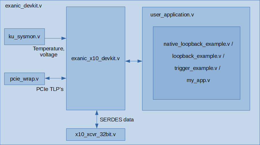
At the top level of the design hierarchy exanic_devkit.v (for SmartNIC K35-S (X10)/SmartNIC K35-Q (X40)) wraps both the SmartNIC IP core netlist
and the custom user application. This top level wrapper provides connections between the
SmartNIC netlist and the user's application. The example designs provide these connections and
can be used as a starting point for adding further functionality.
An overview of the FDK structure for the SmartNIC K35-S (X10) is shown below. Other platforms are similar with slightly different filenames.
Clocking, reset and misc
The user interface has the following clocking and reset signals as inputs:
clk_host(1 bit), a 250 MHz clock generated from the PCIe bus clock. All signals with the_hostsuffix are synchronous to this clock.clk_net(1 bit), orclk_tx_net(1 bit) andclk_rx_net(1 bit per port), depending on the clocking_model selected. Refer to the description of clocking_model above.rst_n(1 bit), an enable line asserted soon after theclk_hostis valid and present. This signal is synchronous toclk_host.
The following optional ports are available depending on the setting of app_ports:
hw_time_net(32 bit), a counter that is shared with the timestamp counter for received packets, having 3.1 ns resolution. This counter is synchronous toclk_tx_net. Note that the host can slew this clock if a PTP client is using a port on this SmartNIC. The utilityexanic-clock-synccan also slew this clock. In both cases, the counting frequency is impacted by the skipping or addition of a cycle periodically.hw_time_host(32 bit), this is simplyhw_time_netcrossed into the host clock domain (clk_host).port_enabled(1 bit per port) indicates that the host OS has enabled the interface. This signal is synchronous toclk_host.port_speed(2 bits per port) indicates the speed that the host OS has configured the port for: 0=Reserved, 1=100M, 2=1G, 3=10G (as of version 2.1.0, port speeds 100M/1G are only fully supported in the SmartNIC K35-S (X10) and SmartNIC K3P-S (X25), on others it is only supported on the first lane of the physical connector - see Netlist Variants). This signal was previously calledrate. It is synchronous toclk_host.link_up(1 bit per port) indicates that the MAC has established a link with the network partner. This signal is synchronous toclk_rx_net. Note that the MAC can take several seconds to establish link.pps_in(1 bit) direct connection from the PPS input pin to the user application.
Register interface
The user register interface allows the user application to implement up to 2048 readable and/or
writeable 32 bit registers. On this interface, reads and writes happen a full 32 bit word at a time,
with no individual byte enables. All signals in this section are synchronous to clk_host. This
interface is implemented using the following signals:
reg_w_en(1 bit), asserted on the same cycle asreg_w_addrandreg_w_datato indicate a register write request from the host.reg_w_data(32 bit), the write data from the host.reg_w_addr(11 bit), the address of the register the host wants to write to. This address increments for each 32 bit word, and is not a byte offset.reg_r_addr(11 bit), the address of the register the host wishes to read. As with the write address, this address increments for each 32 bit word.reg_r_en(1 bit), a read enable signal asserted withreg_r_addrthat indicates the address is valid.reg_r_data(32 bit) is the data for the register selected byreg_r_addr. Data must be provided whenreg_r_ackis asserted.reg_r_ack(1 bit) must be asserted whenreg_r_datais valid in response to a read. The user logic has 16 cycles in which to assertreg_r_ackin response toreg_r_enbefore the read times out. The PCIe logic will reply with an unsupported request response on timeout.
Memory interface
The user memory interface allows the application to implement a write-only (for the host)
memory space. Reading back of this memory by the host is not supported. This can be useful for
the implementation of transmit buffers and maps well to block memories. All writes are
performed synchronous to clk_host. This interface is implemented using the following signals:
mem_w_en(32 bit), 32 bit write byte enable, asserted for each byte offset frommem_w_addrthat the host wishes to write to. The LSB (bit 0) of the write enable signal refers to the byte at offset 0 from the write address.mem_w_addr(19 bit), the memory offset at which the host intends to write to. This is the DWORD offset (32 bit) from the development kit region in BAR2.mem_w_data(256 bit), up to 32 bytes of data (selected by the write enables) that the host wishes to write.
Note that the memory interface is always 'address aligned'. This means that
mem_w_addr[2:0] is always zero, and the byte enables must be used to determine which bytes
will be written to.
The memory region is mapped into the host memory space with both non-cached and write-combining attributes. This means that memory writes may be temporarily stored and combined in the CPU's write combining buffer prior to being sent to the FPGA. Therefore, the sequence of writes seen by the user firmware may not be the same as the sequence of writes performed in software. The total number of writes may change and they may be reordered. You can flush the write buffer by performing a write to the register space from software. If you have backed the memory interface with an FPGA memory, once the synchronizing register write has been received in the user firmware you are guaranteed that the state of your memory is the same as if the writes had been sent to the firmware in program order.
Extra BARs interface
Users may enable additional BARs if the above memory spaces are not sufficient for their application. BAR1 behaves the same as the register space. BAR4 behaves the same as the memory space.
These additional spaces are reserved for the user application only and are not shared with other functions on the card. This means that the user is free to resize and reconfigure the BARs as needed. This is done by editing the relevant .xci file in Vivado. These .xci files can be found in the ip/ directory of the FDK archive.
We provide software and firmware usage examples. See the description of the "extra BARs example" below.
The behaviour of the new signals is the same as the register/memory interface signals above. They are listed below for convenience.
bar1_w_d(32 bit)bar1_w_a1(32 bit)-
bar1_w_en1(1 bit) -
bar1_r_a(32 bit) bar1_r_en(1 bit)bar1_r_d(32 bit)-
bar1_r_ack(1 bit) -
bar4_w_d(256 bit) bar4_w_a(32 bit)bar4_w_en(32 bit)
Network interface
These network-side interfaces allow the user application to send and receive
packets on the network, via the Cisco low-latency MAC. Note that the interface signals
rx_early_sof_net, tx_eof_no_crc_net, and tx_abort_frame_net are only present
in the 10G PCS/MAC and not available for the 100M & 1G PCS/MAC.
The received data is provided via the following signals, all of which are inputs:
rx_data_net(32 or 64 bits per port, depending onnet_data_width). Packet data as received from the wire. The first byte appears at byte 0 (bits 7 to 0).rx_sof_net(1 bit per port), asserted on the same cycle as the first data word received from the wire.rx_data_net[7:0]will contain the first byte of the destination MAC address.rx_early_sof_net(1 bit per port), a 'heads up' that the start of the preamble has been received and thatrx_sof_netwill be asserted in 2-3 cycles. (Only available for 32-bit native mode 10G operations.)rx_eof_net(1 bit per port), asserted on the very last cycle of a received frame. The last bytes seen will include the four byte received CRC.rx_len_net(2 or 3 bits per port, depending onnet_data_width). Asserted on the same cycle as the EOF, indicates how many bytes in the final data signal are valid. As an example, if this reads 1, then only the bottom byte of data (bits 7 to 0) is valid. If it reads 0, then there are no more valid bytes in this cycle and the packet effectively finished in the previous cycle.rx_vld_net(1 bit per port), asserted to indicate that receive data is valid. Due to the overhead of the 64b/66b encoding used in 10G Ethernet, there may be cycles intra-frame that do not contain valid data. This signal only applies torx_data_net. You can assume thatrx_sof_net,rx_early_sof_netandrx_eof_netare always valid and that ifrx_sof_netorrx_eof_netare asserted, then so isrx_vld_net.rx_err_net(1 bit per port), asserted to indicate an abnormal frame termination condition. This can occur when the sender aborts the frame early, or if the link is lost in the middle of a frame. If a frame is terminated withrx_err_net, there will be norx_eof_netfor that frame. This signal is not associated withrx_vld_net. It is possible forrx_err_netto be asserted whilerx_vld_netis low.rx_crc_fail_net(1 bit per port), asserted after EOF to indicate that the frame CRC check failed. For 32-bit datapath this assertion normally occurs two cycles after EOF, but this depends on Cisco build options (see Timing diagrams below). For 64-bit datapath this is provided on the same cycle as EOF (for compatibility with earlier versions of the FDK). For the 32-bit datapath, this signal is not associated withrx_vld_net. It is possible forrx_crc_fail_netto be asserted whilerx_vld_netis low.rx_timestamp_net(32 bit per port), is a counter that serves as the timestamp for the first byte of the received frame with 3.1ns of resolution.
These signals are synchronous to clk_rx_net in native clocking mode, to
clk_net in dual clocking mode, and to clk_host in host clocking mode.
Note that the width of each of the above signals scales with the number of ports. To select the
set of signals for a given port, use bit slicing. For example, RX data for port 0 will occupy
rx_data_net[31:0], and RX data for port 1 will occupy rx_data_net[63:32]. The example designs
show how to perform this bit slicing or indexing for each of the signals on this bus. This note
applies to all of the Ethernet frame interfaces in the FPGA development kit.
Also note that there is no way to apply backpressure. The user application must be able to process packets at line rate.
A transmit interface is also exposed to the SmartNIC development kit application. The user application can monitor and modify frames that are being transmitted by the host, as well as transmit frames of its own. Ethernet frames transmitted by the user application must start with the first byte of the destination MAC address, and end at the last byte of the payload. Logic within the SmartNIC automatically calculates, appends and transmits the CRC. The FPGA application has the following signals which connect through to the Ethernet transmission logic:
tx_data_net(32 bits or 64 bits per port, depending onnet_data_width). The packet data to be transmitted. The first byte that will be placed on the wire (e.g. the first byte of the destination MAC address) is located at bits 7 to 0.tx_sof_net(1 bit per port), to be asserted on the same cycle as the first data word.tx_eof_net(1 bit per port), to be asserted on the same cycle as the last data word.tx_len_net(2 bits or 3 bits per port, depending onnet_data_width), to be set on the same cycle as EOF, indicating the number of bytes of data valid in the last cycle. Likerx_len_net, this may be 0 to indicate that the frame effectively ended in the previous cycle.tx_vld_net(1 bit per port), indicates that the transmit data bus contains valid data. This signal is deprecated and is ignored in native mode, you should not rely on this signal to masktx_sof_net.tx_ack_net(1 bit per port), acknowledge signal provided to the user application. The SmartNIC can be considered to have accepted transmit data from the application for any rising clock edge during which bothtx_ack_netis high and the MAC is currently in the process of transmitting a packet (i.e. between 'sof' and 'eof'). Iftx_ack_netis low all TX MAC interface signals must be held constant. Note thattx_ack_netcan be high outside of packet transmission. This means that, iftx_sof_netis asserted by user logic in the current cycle, then packet transmission will begin immediately. Otherwise it should be ignored.tx_err_net(1 bit per port), corrupt the CRC of the current frame. Note that asserting this signal only corrupts the running CRC calculation, it does not terminate the frame. To terminate the current frame with an invalid CRC, asserttx_eof_netat least one acknowledged cycle after assertingtx_err_net.tx_eof_no_crc_net(1 bit per port), ends transmission of the current frame but does not append the frame checksum. Timing of this signal is the same astx_eof_net. The result of setting bothtx_eof_netandtx_eof_no_crc_netin the same cycle is undefined. If this signal is used, it is the responsibility of the user's firmware to append the CRC to the data stream. (Only available for 32-bit native mode 10G operations.)tx_abort_frame_net(1 bit per port), aborts the current frame without sending an EOF symbol. Timing of this signal is the same astx_eof_net. If the current 64b/66b block is not full when this signal is asserted, the remainder of the block is filled with zeros. (Only available for 32-bit native mode 10G operations.)tx_ifg_compress_net(1 bit per port), Forces the transmitted interframe gap to the smallest value allowed by the deficit idle count algorithm, i.e. when there is no accumulated deficit. Must be set oneofand held constant until thesofof the next frame is acknowledged. In practice, we expect the user will set it to a constant value if they determine that the downstream network device can handle sustained short IFGs. Use with caution.
These signals are synchronous to clk_tx_net in native clocking mode, to
clk_net in dual clocking mode, and to clk_host in host clocking mode.
Note that tx_ack_net may drop out at any time. Also note that, during the frame, valid data must be presented on every cycle. There is no way to stall packet transmission. This is a property of Ethernet, not a limitation of our implementation.
For the 100M and 1G PCS/MAC, asserting the signals that are not supported by
the interface will not cause any harmful effects. Generally, this will also not
result in any useful operations. However, it may be worth pointing out that
asserting tx_eof_no_crc_net will have the same effect as that of tx_eof_net
for 100M and 1G operations.
Timing diagrams
The following timing diagrams highlight edge cases and should clear up any ambiguities in the description above.
The diagram below shows reception of a typical packet. It begins with the sof signal going high and ends with eof. vld may drop out at any time, and, in this case, it drops out in the middle of the packet. Note that data becomes invalid during this cycle. Also note that len is only valid when eof is asserted. The cycle that crc_fail is valid on depends on whether the FDK was build by Cisco with the Extra CRC Reg flag or not. In the case below, the Extra CRC Reg was enabled, so crc_fail is available 2 cycles after eof.

The following timing diagrams demonstrate packet transmission. The diagram below shows transmission of a typical packet. It is very similar to the case for reception, except that the valid signal is replaced with ack. Note that, at the beginning of the packet, sof and the first data word must be held constant until the ack signal is high on a rising edge. Also, ack may drop out anywhere in the middle of the packet, signalling that all signals must take the same value in the next cycle. Lastly, note that ack may be high while a packet is not currently being transmitted. This happens in the first cycle in the waveform below. In this case, ack being high means that the MAC is ready to start packet transmission in the current cycle. This does not imply it will also be ready to begin transmission in the next cycle. If the user firmware asserts sof on this cycle, packet transmission will begin.
![]()
The next set of diagrams illustrate common packet transmission pitfalls and corner cases. Below we illustrate the case where the ack signal is deasserted on the end of frame. As already stated, all signals must remain constant while ack is deasserted. This includes eof, len and ack.

The diagram below demonstrates packet transmission when the size of the last chunk is zero. Since no bytes are valid on the last cycle (when eof) is asserted, the packet effectively ended the cycle before and no valid data bytes are required on this cycle.

Lastly, we demonstrate sending back to back packets. As soon as the end of frame is acknowledged, ack is deasserted, and is kept deasserted by the MAC for several cycles. This is to prevent the user from violating Ethernet's interpacket gap requirements.
![]()
Differences from AXI
Most FPGA engineers are familiar with the AXI stream interconnect. Our MAC interface is very similar to an AXI stream but differs in a few key places for efficiency reasons. Aside from the naming of signals, this section explains the differences.
RX side:
- There is an extra signal:
rx_sof_net. This signal is redundant and it is possible to rely only onrx_vld_netto determine when a packet starts as it will be the first time it goes high after an end of frame. - The
rx_len_netsignal is encoded as a binary number instead of as a bitmask (tkeepin AXI). Since we can't have arbitrary bytes in a chunk invalid, a bitmask doesn't make sense. This is consistent with the DMA engine interface.
TX side:
- As above,
tx_len_netis also encoded as a binary number. - There is no valid signal to the MAC. We chose not to provide a valid signal because that would incorrectly imply the user can set valid to false mid packet. Instead
tx_sof_netis used to signal that the first chunk is valid. From then on, the data is required to be valid until the end of frame.
Host interface
The host-side interface allows the user application to forward packets to host software, or to receive packets that have been sent from host software.
The bus semantics are intentionally similar to those on the network side, with
_net replaced by _host. Thus, forwarding packets to the host can be done
by connecting the rx_*_net bus to the rx_*_host bus, and forwarding packets
to the network can be done by connecting the tx_*_host bus to the tx_*_net
bus. Doing this producing a 'null' application which functions as a normal
network interface adapter. More interesting applications can be built by
interceding between these transfers in various ways. (Note, depending on the
clocking model selected, clock domain crossings [asynchronous FIFOs] may be
required.)
The receive side host signals (all in the clk_host clock domain) are:
rx_data_host(64 bits per port), the packet data to be sent via PCI Express. The first byte (e.g. the first byte of the destination MAC address) is located at bits 7 to 0.rx_sof_host(1 bit per port), to be asserted on the same cycle as the first data word.rx_eof_host(1 bit per port), to be asserted on the same cycle as the last data word. bytes seen will include the four byte received CRC.rx_len_host(3 bits per port), to be asserted on the same cycle as the EOF. Indicates how many bytes in the final data signal are valid. As an example, if this reads 1, then only the bottom byte of data (bits 7 to 0) is valid. If it reads 0, then there are no more valid bytes in this cycle and the packet effectively finished in the previous cycle.rx_vld_host(1 bit per port), to be asserted when the above signals are valid. Can be used to mask validity.rx_err_host(1 bit per port), can be asserted to abort the frame prematurely (software receives EXANIC_RX_FRAME_ABORTED). Ifrx_err_hostis asserted,rx_eof_hostdoes not need to be asserted (and should not be).rx_crc_fail_host(1 bit per port), asserted at EOF to indicate that the frame CRC check failed (software receives EXANIC_RX_FRAME_CORRUPT). Normally connected torx_crc_fail_netfor forwarded frames, or to 0 if frames are generated internally in logic.rx_timestamp_host(32 bit per port), can be used to provide a hardware timestamp for the packet. (Normally this should be sourced fromrx_timestamp_netorhw_time_host.) The correct value for this port should be set when the 14th valid data beat is applied to therx_data_hostinterface, or at the cycle beforerx_eof_hostis asserted, whichever occurs first. Once set it should be kept constant untilrx_eof_hostis asserted.
There are two additional signals that are not in the _net bus:
rx_match_host(8 bit per port), allows the user application to tag frames with an 8 bit code with application specific meaning. This code will be provided in the information section of each chunk of the frame that is transferred to the host.rx_buffer_host(6 bit per port), allows the user application to steer frames to different userspace buffers on the host system. This signal can also be used to filter and drop frames before they get to the host. For more information on custom flow steering, see the flow steering example design section of this document.
The value applied by the user application to these ports must be ready at the same time as the 15th valid data beat is applied to the corresponding rx_host interfaces, or at the end of frame, whichever occurs first. Once set, this value must remain the same for the duration of the frame until EOF+2 cycles.
Note
A minimum of 1 spare cycle is required between EOF and SOF being asserted. Normally frames coming off the wire will have at least this (even at full line rate, due to ethernets minimum Inter-Frame Gap). However if the user application is generating frames to send up to the host in addition to those coming off the wire then this requirement must be observed by the user logic.
With SmartNIC K35-Q (X40)/SmartNIC+ V9P platforms, we ship additional variants that has wider per port bandwidth in the host-side interface. In these netlists, the width of rx_data_host is 256 bits instead of 64 bits as in other netlists. With 256 bit interface, the bandwidth from SmartNIC IP core to the PCIe core would be same as in 64 bit netlists. But, this interface allows user application to send data to the SmartNIC IP core at a higher bandwidth.
The 256 bit receive side host signals (all in the clk_host clock domain) are:
rx_data_host(256 bits per port), the packet data to be sent via PCI Express. The first byte (e.g. the first byte of the destination MAC address) is located at bits 7 to 0.rx_sof_host(1 bit per port), to be asserted on the same cycle as the first data word.rx_eof_host(1 bit per port), to be asserted on the same cycle as the last data word.rx_len_host(5 bits per port), to be asserted on the same cycle as the EOF. Indicates how many bytes in the final data signal are valid. If it reads 0, then there are no more valid bytes in this cycle and the packet effectively finished in the previous cycle.rx_vld_host(1 bit per port), to be asserted when the above signals are valid. Can be used to mask validity.rx_err_host(1 bit per port), can be asserted to abort the frame prematurely (software receives EXANIC_RX_FRAME_ABORTED). Ifrx_err_hostis asserted,rx_eof_hostdoes not need to be asserted (and should not be).rx_crc_fail_host(1 bit per port), asserted whenrx_eof_hostis asserted to indicate that the frame CRC check failed (software receives EXANIC_RX_FRAME_CORRUPT).rx_timestamp_host(32 bit per port), can be used to provide a hardware timestamp for the packet. The correct value for this port should be set when the 2nd valid data beat is applied to therx_data_hostinterface.rx_match_host(8 bit per port), allows the user application to tag frames with an 8 bit code with application specific meaning. This code will be provided in the information section of each chunk of the frame that is transferred to the host. The correct value for this port should be set when the 4th valid data beat is applied to therx_data_hostinterface, or at the cycle in whichrx_eof_hostis asserted, whichever occurs first.rx_buffer_host(6 bit per port), allows the user application to steer frames to different userspace buffers on the host system. This signal can also be used to filter and drop frames before they get to the host. The correct value for this port should be set when the 4th valid data beat is applied to therx_data_hostinterface, or at the cycle in whichrx_eof_hostis asserted, whichever occurs first.rx_afull_host(1 bit per port), asserted by SmartNIC IP core to indicate that there's only 1600 bytes of space remaining in the SmartNIC IP core's internal buffer to whichrx_data_hostdata is written. If the internal buffer runs out of space, host could receive corrupted data. Therefore, user should not start any new data transfers whenrx_afull_hostis asserted.
The transmit side host signals (all in the clk_host domain) are:
tx_data_host(64 bits per port). Packet data as received from the host. The first byte appears at byte 0 (bits 7 to 0).tx_sof_host(1 bit per port), asserted on the same cycle as the first data word received from the host.tx_data_host[7:0]will contain the first byte of the destination MAC address.tx_eof_host(1 bit per port), asserted on the very last cycle of a received frame. The received frame from software will not include the CRC.tx_len_host(3 bits per port). Asserted on the same cycle as the EOF, indicates how many bytes in the final data signal are valid. As an example, if this reads 1, then only the bottom byte of data (bits 7 to 0) is valid. If it reads 0, then there are no more valid bytes in this cycle and the packet effectively finished in the previous cycle.tx_vld_host(1 bit per port), asserted to indicate that the data bus is valid. The above signals should only be acted on iftx_vld_hostis asserted (i.e. it should be used as a clock enable).tx_ack_host(1 bit per port). Stalls the port transmit engine when low. The same data word is re-presented untiltx_ack_hostis asserted high. This can be connected totx_ack_netwhen transmitting the packet to the network, or asserted whenever a stall is required by user logic.
Normally, the SmartNIC DMA engine will pad frames sent down from host software that are below
the minimum frame size (<64 bytes). The user application can elect to disable this padding on a
per port basis by asserting the disable_tx_padding flag. The flag is sampled
at each SOF, but note that it will not apply until the next frame - it is not
possible to dynamically change the padding setting depending on frame contents.
The example designs provide code that shows how to multiplex FPGA generated frames with the
host data path, using the provided vabus_mux module.
DDR interface
The DDR interface provides read and write access to DRAM installed on the card. Note that not all SmartNICs have DRAM installed:
- SmartNIC+ V5P: ships as standard with 9GB of DDR4 DRAM
- SmartNIC+ V9P: ships as standard with 9GB of DDR4 DRAM
- SmartNIC K3P-S (X25): can optionally be supplied with 4GB of DDR4 DRAM
- SmartNIC K3P-Q (X100): can optionally be supplied with 9GB of DDR4 DRAM
- All other cards: DDR not available.
Note
For most signals, more detailed information (including waveforms) can be found in the Xilinx documentation for Ultrascale+ Memory IP (PG150).
The DDR interface consists of three sets of signals: signals for reading, signals for writing, and signals shared between reading and writing. The signals shared between reading and writing are as follows:
c0_ddr4_ui_clk: input. This is a 161MHz clock that must be used for all interactions with the other DDR signals.c0_ddr4_ui_clk_sync_rst: active-high, input. This indicates that any logic in the user application related to DDR should be reset.ddr_npres: active low, input. This indicates whether DRAM is physically present.ddr_reset: active high, output. Asserting this signal will cause all DDR logic on the card (and the DRAM itself) to reset.c0_ddr4_ui_clk_sync_rstwill also get asserted as part of this process.c0_init_calib_complete: active high, input. Indicates that the DDR module has finished its startup procedure. This signal is level-triggered, i.e. it will stay high once calibration is complete.c0_ddr4_app_rdy: active high, input. Indicates that the DDR user interface is ready to accept commands. If this signal is deasserted whilec0_ddr4_app_enis high, then the current values ofc0_ddr4_app_en,c0_ddr4_app_addr, andc0_ddr4_app_cmdmust be held constant.c0_ddr4_app_en: active-high, output. This is a strobe forc0_ddr4_app_addrandc0_ddr4_app_cmd.c0_ddr4_app_addr: 30 bits, output. This is the address for the current request.c0_ddr4_app_cmd: 3 bits, output. This is the command for the current request. Allowed values are3'b000for write requests and3'b001for read commands.
Signals that apply only to read requests are as follows:
c0_ddr4_app_rd_data_valid: active high, input. Indicates thatc0_ddr4_rd_datais valid.c0_ddr4_app_rd_data: 256 bits, input. Provides the output data from read commands.c0_ddr4_app_rd_data_end: active high, input: Indicates that the current clock cycle is the last cycle of output data onc0_ddr4_app_rd_data.
Signals that apply only to write requests are as follows. Note that wdf
stands for "write data FIFO", and is reused from the Xilinx memory IP
interface.
c0_ddr4_app_wdf_rdy: active high, input. Indicates that the memory interface is ready to receive data.c0_ddr4_app_wdf_wren: active high, output. Strobe forc0_ddr4_app_wdf_datac0_ddr4_app_wdf_data: 256 bits, output. Provides the data for write commands.c0_ddr4_app_wdf_mask: 32 bits, output. Provides a byte-keep mask forc0_ddr4_app_wdf_data. It prevents corresponding bytes from being updated.c0_ddr4_app_wdf_end: active high, output. Indicates that the current clock cycle is the last cycle of output data onc0_ddr4_app_wdf_data.
Note
Previous versions of the DDR interface for included some signals
that have since been removed since they were reduntant. These
signals are: dbg_clk, dbg_bus, c0_ddr4_app_hi_pri, and
addn_ui_clkout1. It is also the case that the memory interface for
the SmartNIC+ V5P is now controlled with the ddr parameter in app_ports
(see above) rather than editing the supplied files in the FDK.
Software integration
Low level
The user application can interface with software via its address space, as well as via modifying and tagging received packets prior to them being transferred to the host. In the first instance, pointers to the register and memory address space can be obtained using libexanic, calling:
exanic_get_devkit_registers()to get a pointer to unsigned 32 bit values the register space, andexanic_get_devkit_memory()to get a pointer to byte values in the memory space.
The value and meaning of the registers and memory in these address spaces are dependent on the user's FPGA application.
Utilities for reading and writing to the user register space are provided in the examples/devkit directory of the exanic-software source package.
For example, in trigger_example.v of the FDK, the registers are defined like so:
/* Register reads. */
always @ (posedge clk_host) begin
  reg_r_ack <= reg_r_en;
  case (reg_r_addr)
    'h0:    reg_r_data <= FIRMWARE_ID;
    'h1:    reg_r_data <= VERSION;
    'h2:    reg_r_data <= armed;
    'h4:    reg_r_data <= match_length;
    ...
    ...
FIRMWARE_ID is defined to be 32'hEB000001, so reading register 0 yields:
$ ./exanic-devkit-register-read exanic0 0
0x000: 0xEB000001 (-352321535)
The user application can also communicate with the host via dummy ethernet frames. An example of this is shown in the ping example application, where a dummy frame with a custom ethertype is DMA transferred to the host. This frame is received using libexanic and contains user-defined data.
TCP stack integration
The SmartNIC driver package includes support for exasock extensions. These extensions allow applications to obtain the next set of TCP headers for a particular socket. When used in conjunction with the development kit, these functions allow the host to manage TCP state (through transparently bypassed kernel sockets, via exasock) and allow the card to send 'fast' responses in response to user defined events.
Within the driver source tree, the exasock-tcp-responder-example.c example application
shows how to use these functions with the trigger example firmware. This example shows how
normal UNIX socket calls can be used to make a TCP connection to a server, with the card
sending a TCP reply in response to a received UDP packet.
Included cores
The SmartNIC FPGA development kit ships with source code for IP cores that are useful for performing common tasks.
Field extract (field_extract.v)
The field extract core can be used to extract an arbitrary length field from received frames. To use the core, instantiate it by specifying the following two parameters:
- BYTES: The byte width of the field to extract.
- OFFSET: The offset in bytes of the field in the frame, measured from the start of the frame.
The core can be wired directly to the development kit frame interfaces via its data, sof and vld
inputs. The field extract core will strobe the field_vld output for one clock cycle when the field
output contains the value of field in the currently received frame.
Examples of using this core are shown in the ping and flow steering example applications.
Frame mux (frame_mux.v)
The frame mux core provides a way to share a single frame output interface (for example,
rx_host or tx_usr) between two sources of frames. It provides buffering so that interfaces that
cannot be 'stalled', such as the receive interface, can be arbitrated without loss of data. A
typical application is shown in the ping example application, where the
frame mux is used to share the host DMA datapath between received frames and FPGA generated frames.
The frame mux also allows two ports to be 'bridged' together, much like the SmartNIC bridging functionality. As an example, the frame mux can be used to connect port 0 receive to port 1 transmit, whilst also allowing the host to transmit via port 1. In this mode of operation, the frame mux has an optional FCS removal mode. This is required because received packets are provided to the user application with the FCS present, however the FCS must be removed prior to passing them to the transmit interfaces.
The frame mux core has the following parameters:
- DEPTH: The total buffering depth of the two FIFOs contained within the frame mux. This is the maximum number of QWORDs that the frame mux can store.
- IN0_DELAY, IN1_DELAY: The amount of 'prebuffering' to apply to a particular input of the mux, prior to providing it to the output. This is useful when connecting the receive of one port to the transmit of another, since Ethernet clock mismatch may result in transmitter starvation unless enough of the packet is available in a buffer prior to beginning the transmit process.
- STRIP_FCS0, STRIP_FCS1: selects whether to remove the last 4 bytes from a particular input. Useful for removing the FCS from a received packet prior to transmitting it out another port.
Valid/ack bus mux (vabus_mux.v)
The valid/ack bus mux core provides the same functionality as the frame mux core but without any buffering or registering delays. This is useful where latency is important. A typical application is the muxing of custom transmit logic together with the normal SmartNIC transmit logic. This use case is shown in both the trigger and ping examples.
Custom framegen (custom_framegen.v)
The custom framegen core generates a custom, broadcast, ethernet frame, that contains 4 QWORDS that are set by inputs to the module. This is useful for generating packets on the card and sending them to the host application. An example of this is shown in the ping example application, where the custom framegen core is used to send timestamps to the host.
The CUSTOM_ETHERTYPE parameter to the module allows the user to specify the ethertype of the frame. Setting the ethertype to a non-standard value will result in normal kernel processes safely ignoring the packet.
Asynchronous FIFO (async_fifo.v)
The asynchronous FIFO provides fast clock domain crossing between two domains. Data is
written into the the FIFO synchronous to clk_write when wren is asserted by the user, provided
the FIFO is not asserting full.
Data is read from the FIFO synchronous to clk_read, on any cycle when vld and rden are both
asserted.
Flag Synchronizer (flag_sync.v)
The flag sync module is used to cross a single bit flag between two asynchronous clock domains. The flag should be asserted for a single cycle in the input clock domain. Internal logic will then safely cross this flag such that it will then be asserted for a single cycle in the output clock domain. Note that this module assumes that the flag will be asserted relatively infrequently in the input clock domain.
Asymmetric memories (ram_256_32.v and ram_256_64.v)
The asymmetric memories provide block ram backed 256 bit write and 32 bit or 64 bit read capability. They are intended for designs where packet data is received from the 256 bit PCI memory write interface and sent out one of the network interfaces.
Stream pipeline (stream_pipeline.v)
The stream pipeline module is used to break up long timing paths that stream data with valid and ack signals. Timing paths are broken in both the forward and reverse (ack) directions. It is particularly useful when transferring data between Ethernet and PCI which, on the SmartNIC+ V5P, are at opposite ends of the chip.
Streaming bus width conversion (shim_32_to_64.v and shim_64_to_32.v)
These modules can be used to convert between the streaming interfaces of the MAC and DMA engines, which have different data widths.
Example designs
The full source code is provided for all of the example applications described in this section. In all of the following examples a convention is used whereby register zero (0) in the development kit register address space reports a 'firmware ID'. This firmware ID is read by the software side of the example to verify that the correct firmware is running on the SmartNIC.
Trigger example
The trigger example application allows users to pre-load the card with a pattern, mask and reply frame. The application performs a match on port 0 of any incoming frame against the pattern and mask, and if a match occurs the application will transmit the reply frame. This application can be used as a starting point for more advanced custom logic.
All source code for this application is included in the src/trigger_example directory of the
development kit package. The files include:
- ram_256_64.v, which implements a block RAM interface compatible with the development kit memory addressing scheme.
Two sample C applications for interfacing with this application is provided in the SmartNIC driver
package, under examples/devkit in the ExaNIC software.
One example, libexanic-responder-example, shows how
to use the low level API to preload the card with a frame. The other, exasock-tcp-responder-example
shows how to use Exasock extensions to integrate the host TCP state with the FPGA
application.
In both of these applications software application primes the FPGA trigger to match on incoming IP frames, and loads in a dummy reply. The application reports any time the FPGA logic has triggered. The libexanic application can be started using
$ ./libexanic-responder-example exanic0
The exasock example will attempt to connect to the specified TCP address/port combination. Once a connection has been established, any UDP packet that is received on the UDP port will trigger a 'hello world' packet to be sent via the TCP connection. The exasock application can be started using:
$ exasock ./exasock-tcp-responder-example <udp-port> <tcp-addr> <tcp-port>
Note that the example application is only implemented on the FPGA for port 0, and all ports operate as normal network interfaces.
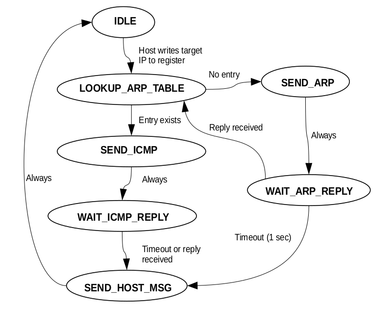
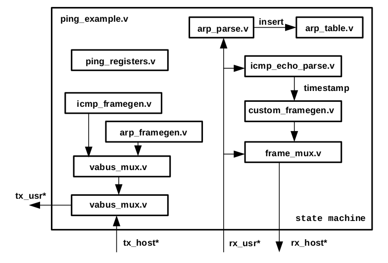
Ping example
The ping example uses an ICMP echo request to perform a hardware timestamped ping. The firmware takes a source IP address and destination IP address. This triggers a state machine to start by checking an ARP table for an entry that resolves the remote IP to a MAC address. If no entry for the IP address is found, the hardware sends an ARP request for the IP out on the wire and waits for a reply. When an ARP reply is received, an entry is inserted into the ARP table and the ARP table lookup performed again. The hardware then sends an ICMP echo request, filling the body of the request with a hardware timestamp, then waits for a reply. When the reply is received, the hardware sends a custom frame to the software application that contains the transmit and receive timestamps. Both ICMP and ARP requests have timeouts of 1 second associated with them, and will result in an error message sent to the host on timeout.
The ping example demonstrates the following functionality within the devkit:
- Sending pre-defined packets with values of certain fields substituted with values calculated in the FPGA. This is demonstrated in the ARP framegen and ICMP framegen modules.
- Parsing received packets and extracting information from them. The ICMP echo parse and ARP parse modules demonstrate this functionality.
- Communicating with the software application by sending a custom frame from the FPGA via the DMA interface. The custom framegen module and frame mux modules demonstrate how to interleave custom frames with frames that are received from the wire.
- Basic lookup table example (ARP table).
- Use of hardware timestamping functionality.
To run the ping example, use:
$ ./ping-example <device> <dst-ip> <src-ip>
This will send ARP and ICMP packets originating from src-ip to the host at dst-ip. The
device must be a SmartNIC with the ping example firmware loaded.
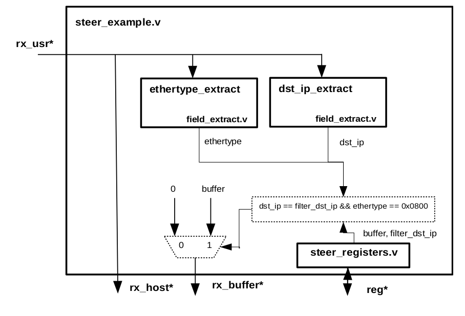
Flow steering example
The devkit can be used to perform flow steering based on any field within an ethernet frame. The raw frame API, libexanic, can be used to allocate DMA buffers, each of which is automatically assigned a unique ID. This ID can be passed to the card and provided to the RX host interface in conjunction with the frame in order to steer the frame to that buffer. Applications include per-symbol filtering of market data or more advanced, stateful filtering.
The flow steering example provided in the devkit demonstrates how to use this functionality to steer IP packets destined for a particular IP address to a designated buffer. Applications that monitor this buffer will only see packets that are destined for this IP address. Users can adapt this application to their requirements.
The rx_buffer_host port in the devkit can be used to pick the host receive buffer that the current
frame is sent to. The value applied by the user application to this port must be ready at the
same time as the 15 th valid data beat is applied to the corresponding rx_host interfaces, or at
the end of frame, whichever occurs first. Once set, this value must remain the same for the
duration of the frame until EOF+2 cycles.
The rx_buffer_host port can also be used to filter and drop frames before they are sent to the host.
If all the bits in rx_buffer_host are set to 1, the frame will be dropped before it is received by any
of the buffers. The bits of rx_buffer_host should be set to 1 by the time 15 th valid data beat is applied
to the rx_host interface or at the end of the frame, whichever occurs first.
Bridging example
The bridging example demonstrates the use of the frame mux for bridging of two ports on the card. Bridging involves looping back any received data on one port to the transmit datapath on another port. Note that this example will not work when a different line rate is used on each side of the bridge as there is no buffering added.
Soft responder
The soft responder example demonstrates the latency of the SmartNIC MAC layer. It does this by sending a packet out of port 0 as soon as the start of frame is seen on the RX datapath of port 0. Note that this demo logic just sends a small frame of all 0xFF's (plus CRC).
Native loopback example
The native loopback example also demonstrates the latency of the SmartNIC MAC layer, but loops back the frames received from the RX datapath on port 0 back out of port 0. This includes a CDC to transfer data from the receive domain to the transmit domain and also 3 cycles of buffering to prevent TX underrun issues.
Chipscope example
The chipscope example also demonstrates the latency of the SmartNIC MAC layer, albeit in the opposite "direction" to the loopback example - instead of sending incoming packets out of another port, it acts as a partial NIC. The intended usage of this example is to connect a loopback cable from port 0 to another physical port.
The default RX port is 0 and the default TX port is 1. Note that for the SmartNIC K35-Q (X40)
and SmartNIC+ V5P, you'll need a different type of cable to test this configuration,
as ports 0 and 1 are in the same QSFP cage. It may be easier instead to
change the TX and RX ports to 0 and 4 in config.tcl when testing on an SmartNIC K35-Q (X40)
or SmartNIC+ V5P, so that a plain QSFP cable can be used.
The default set of signals observed is:
tx_data_nettx_len_nettx_sof_nettx_eof_nettx_vld_netrx_data_chipscoperx_len_chipscoperx_early_sof_chipscoperx_sof_chipscoperx_eof_chipscoperx_vld_chipscope
The TX signals are straightforward - they are the exact signals that get sent to the MAC. The RX signals are the signals received on port 0, after they've been crossed from the RX clock domain to the TX clock domain. This is required since a given ILA can only sample on a single clock domain. This adds a small, non-deterministic amount of latency between one and two clock cycles.
Note that when viewing signals in Chipscope, signals over one bit wide may be
split into several component signals. For example, the tx_data_net signal may
appear as a combination of tx_data_net[19:0], tx_data_net[22:20] and
tx_data_net[63:23].
Multi preload tx example
The multi preload tx example allows the user to preload frames into the memory of the FPGA and then send them out several ports simultaneously in response to a single register write.
Each port has its own packet memory capable of holding 32 2048 byte packets. Additionally, each port has a smaller metadata ram for storing the size of each of the 32 packets as a 16 bit number. The per-port packet buffers are completely independent.
Every byte in each port's packet buffer is individually writable. This means that software can update key fields in the packet individually as needed.
To send a packet, the controlling software writes a single 32 bit value to address 0x0 in the devkit register space. The value is structured as follows:
[24 bits of port mask] [3 unused bits] [5 bits of index]
The index tells the firmware which of the pre-formatted packets to send. The 5 bits of index allows up to 32 different packets to be addressed. Note that, since the per-port packets buffers are separate this design is capable of sending different packets down different ports in response to a single register write.
The port mask tells the firmware which ports to send on. For example, a value of 0x3 would instruct the firmware to send packets on only ports 0 and 1.
In addition to sending predefined packets in response to a trigger, this example also behaves as a normal NIC. You can send and receive packets using the usual DMA interface.
Software to drive this design is available in the exanic-software repository at examples/devkit/exanic-devkit-multi-preload-tx-example.c.
Note that the regular libexanic TX API can also precache packets to be triggered later. The advantage of this design is that you can send packets out multiple ports simultaneously. If you only need a single port, we recommend you use the libexanic API.
Native register example
This is a minimal example of how to use the PCI register interface at BAR0. The memory interface at BAR2 is similar.
Native spam example
This is a simple packet generator for transmitting closely spaced frames of varying sizes. It can be configured by host software using the PCI register interface.
Software to drive the packet generator is available in the exanic-software repository at examples/devkit/spam-example.c. Example usage:
$ ./spam-example -c 100 -s 60 -S 80 -g 0
This will send 100 frames with sizes 60 to 80 back to back.
Note that if the -c argument is not provided, it will send frames forever.
Extra BARs example
This is a minimal example of how to use the additional register/memory spaces at BAR1 and BAR4. Software to drive this example is available in the exanic-software repository at examples/devkit/exanic-devkit-extra-bars-read.c and examples/devkit/exanic-devkit-extra-bars-write.c. For example, to read from offset 0 in BAR1 from a device at PCI address 01:00.0:
$ ./exanic-devkit-extra-bars-read /sys/bus/pci/devices/0000\:01\:00.0/resource1 0
Testbench and functional model
The SmartNIC development kit is provided with a full functional model for all of the individual
interfaces. This can be found in the tb/ directory of the package. The testbench consists of the
following files:
bench.v,the top level harness that wraps the various modules contained in the functional simulation.address_access.v, contains tasks that simulate access to the BAR0 and BAR2 memory spaces in the development kit (for example, register access and memory copies).control.v, contains various control tasks and generates the timestamp counter.dma_sim.v, simulates the SmartNIC frame DMA interface. Will log frames that have been transferred successfully, and indicate error conditions.transmit_sim.v, simulates the SmartNIC ethernet transmit interface. Will log frames that have been transferred successful and indicate error conditions.frame_sim.v, simulates either host frame transmission or frames received from the wire.frame_sim_32bit.vworks the same asframe_sim.v, but for the 32-bit datapath (as used in e.g. native clocking mode).test_cases.v, container for user test cases. Users can add their own simulation directives here.bench.prj, a project file for the Xilinx simulator that lists all files that make up the simulation. New files for a project should be added here to make sure they are picked up by the simulator.start_sim.sh, a shell script that starts the Xilinx simulator in console mode. To start in graphical mode, use the switch -gui.
The example in test_cases.v shows how users can exercise the various elements of the
functional mode, and provides a test case for the example design. Users can add their own test
cases to this file as necessary.
Users can start the example testbench by running:
$ ./start_sim.sh
This will cause the testbench to be compiled and xsim to start in command line mode. From the xsim prompt, the simulation can be run for 10 microseconds by entering:
% run 10us
Debugging with Vivado
You can use Xilinx Chipscope Pro Integrated Logic Analyzer (ILA) to debug your FPGA designs using JTAG. Xilinx documentation on how to use Chipscope for debugging can be found here.
The default build of the chipscope_example includes a Chipscope core to probe
several relevant signals, see the documentation for the Chipscope example
for more details. It is also worth reviewing the debug_clk configuration
option.
The definition of any signals to be probed must include the tag (* mark_debug="true" *).
A TCL script can be used to insert the ILA core to the netlist. In the given
example, debug.tcl is sourced to insert the core. The signals will be captured
with respect to a clock which is specified by the user using the debug_clk
configuration option. Any signals that include the tag (* mark_debug="true" *)
will be captured.
Using the ILA can be done through a local or remote JTAG connection, as described below.
Remote JTAG Connection (XVC Server)
Xilinx supports a remote connection from Vivado to a server using Xilinx's Virtual Cable XVC protocol, which then connects to the FPGA. Cisco has a modified version of Xilinx's xvcServer utility that can be used with SmartNICs.
In order to support JTAG over XVC, some logic needs to be added to the design. Users should add the flag JTAG=1 to the make command when building FDKs to add this logic. NOTE that the addition of this logic instantiates a MASTER_JTAG primitive in the design, which then disables the external JTAG interface. If external JTAG access is required again, it is necessary to revert to an image without the JTAG redirection (either by flashing a new image with exanic-fwupdate, or by using the recovery button).
Build and run the exanic-xvcserver utility, which can be found in the examples/devkit directory of the exanic-software repository:
$ sudo ./exanic-xvcserver exanic0
Waiting for connection on port 2542...
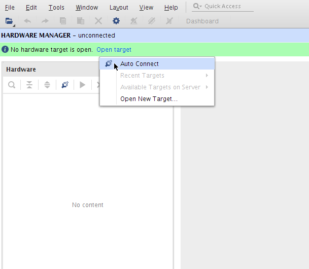
In Vivado, open the Hardware Manager as shown below. Note you can also use the Tcl command open_hw.
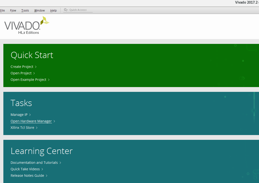
Start a Hardware Server session with the following command on Tcl Console connect_hw_server or by selecting Open Hardware Manager from the Flow menu.
In the Tcl console, issue the open_hw_target command to connect to the machine running exanic-xvcserver. For example:
open_hw_target -xvc_url 172.16.0.210:2542
exanic-xvcserver should report connection accepted and the xcku035_0 device should be listed in Vivado.
If your design has an ILA core, in the Trigger Setup window for the ILA core, click on the link to specify debug probes and select the .ltx probes file which will be in the outputs/ directory.
Note
Cisco has seen instances where MIGs and ILA cores are not listed under the xcku035_0 device alongside SysMon. If you expect to see a core and don't, right click on the xcku035 device and select refresh.
Warning
Users should not attempt to configure the FPGA using the XVC server, as this relies on the FPGA to be configured to handle the JTAG shift instructions.
NOTE that exanic-xvcserver detects whether the JTAG logic has been inserted into the design and will not attempt to connect to an exanic without it.
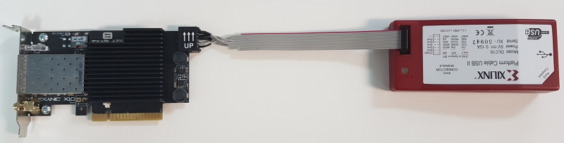
Local JTAG Connection (Xilinx Platform Cable)
The Xilinx Platform Cable can be used for connecting via JTAG to the SmartNIC K35-S (X10) and SmartNIC K35-Q (X40). Connect one end of the Platform Cable to the machine running Vivado, and the other end to the SmartNIC.
There is a small edge connector on the top right corner of the SmartNIC K35-S (X10) and SmartNIC K35-Q (X40) that exposes the JTAG pins, and an adapter cable can be supplied by Cisco to connect the SmartNIC to the Platform Cable.
The SmartNIC+ V5P has 2 methods for connecting to the device with a local JTAG connection. Refer to this page for further details.
In Vivado, open the Hardware Manager as shown above.
Start a Hardware Server session with the following command on Tcl Console connect_hw_server or by selecting Open Hardware Manager from the Flow menu.
Then click on Open target and then Auto Connect.
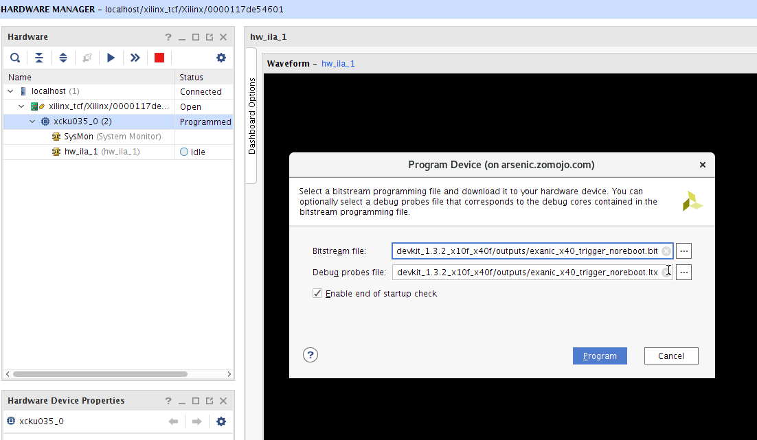
You should now see the xcku035_0 FPGA listed. In the Trigger Setup window for the ILA core, click on the link to specify debug probes and select the .ltx probes file which will be in the outputs/ directory.
Using JTAG to configure the FPGA
The recommended method for configuring the FPGA is to load the image/bitfile using the exanic-fwupdate utility, however configuration via JTAG is possible. The default behaviour of the SmartNIC is to reconfigure the FPGA when the host is reset. When loading on an image via JTAG, it's important to disable this automatic reboot mechanism, otherwise the image that's in flash will be reloaded into the FPGA.
This is done by adding the NOREBOOT=1 flag when building the image:
make PLATFORM=x40 TARGET=trigger NOREBOOT=1
Connect to the FPGA via JTAG using the Xilinx Platform Cable. Users should not attempt to configure the FPGA using the XVC server.
Right click on the Xilinx device and click Program Device.
Booting from flash while JTAG cable is connected
There is a known issue in Vivado where booting from configuration flash can occasionally fail when a JTAG cable is connected and Vivado HW Manager is open. This can unexpectedly leave the FPGA device unprogrammed. According to Vivado Programming and Debugging User Guide (UG908) v2019.2:
When the Hardware Manager polling and recover feature interrupts the Master mode configuration, intermittent configuration failures occur on power up. To avoid this issue, set the following parameter in the Vivado Hardware Manager Tcl console to ensure that the configuration status registers are not updated:
set_param xicom.allow_cfgin_commands false
Please note that when this parameter is set to false, automatic updates of configuration status registers for all of the devices in the JTAG chain are disabled and as a result, the values of registers such as REGISTER.CONFIG_STATUS and REGISTER.BOOT_STATUS shown in Vivado HW Manager are outdated. In order to read the correct updated values for these registers, this parameter needs to be re-set to true using set_param xicom.allow_cfgin_commands true after the bootup is complete and then the relevant device needs to be refreshed (using refresh_hw_device [get_hw_devices <device_name>] in Vivado HW Manager Tcl console, or by right-clicking on the device and selecting Refresh Device).
Netlist variants
There are several build options that are available for the FDK that Cisco needs to set at the FDK build time, rather than at the customer's build time. This is handled by netlist "variants". For each variant that Cisco has built, there is a .edn netlist in the src/ directory of the FDK.
User can select the variant to be used in an application by setting the variant flag when running make. For example, in order to build a native_loopback_example for the SmartNIC+ V5P, using the full variant:
$ make PLATFORM=v5p TARGET=native_loopback_example VARIANT=full
As of 2.7.0, the following variants currently ship in full FDKs:
- full: default build options (10G only)
- full_multirate: built with 100M/1G as well as 10G support (1 extra cycle of latency)
- full_multirate_extrarxreg: adds an additional pipeline stage in the RX MAC to ease timing
- full_txbuf16: built with 16KB instead of 32KB TX buffers to save BRAMs
- full_fastmac (SmartNIC+ V5P only): extra fast MAC to save an additional 3-6ns
- full_ate_fastmac (SmartNIC+ V5P only): additionally includes Accelerated Transmit Engine
The same variants are also available for evaluation FDKs (replace "full" with "eval"). For free FDKs, there is only one variant currently available, which does include 100M/1G support, but not ATE or FastMAC or other features.
Note
Currently 100M/1G is only enabled for the first lane of each physical connector on a SmartNIC, when using a multirate variant. This means that 100M/1G support will only be enabled on port 0 and 4 of the SmartNIC K35-Q (X40)/SmartNIC+ V5P, while the SmartNIC+ V9P will only support 100M/1G on ports 0 and 8. The SmartNIC K35-S (X10) and SmartNIC K3P-S (X25) can support 100M/1G on both physical ports if using a multirate variant.
Ports which do not have 100M/1G enabled can only operate at 10G.
Recovery image
All SmartNICs come with a recovery flash image
for cases where a corrupt flash image has been written to the card. To start
the card in recovery mode, hold down the small button marked 'recovery' located
on the top edge of the card during a reboot of the host system. On the SmartNIC K35-S (X10), the
red LED on the rear panel of the SmartNIC will then be lit. On the SmartNIC K35-Q (X40) and SmartNIC+ V5P
cards, the link lights will flash in an alternating amber colored pattern. When
in recovery mode, the corrupt flash image can be overwritten by using the
exanic-fwupdate utility.
Remote recovery procedure
If it is not possible to physically access a SmartNIC to perform the standard recovery procedure, may be possible to remotely recover a SmartNIC via Vivado by directly writing to the configuration flash. There are 2 prerequisites for this:
- The SmartNIC must be connected via JTAG
- The image currently programmed must not have been built with JTAG=1
If these conditions can be met, then the remote recovery procedure can be performed as follows:
- In Vivado, connect to the FPGA via JTAG.
- Right click the FPGA device, go to "Add configuration memory device".
- You will need to select the appropriate memory part device for the SmartNIC in use. These are available in the table below.
- Vivado will then prompt you to program the memory, select an .mcs file of a known-good firmware build. Typically, a build of native_nic_example can be used for this purpose. OK-ing all of the following prompts will cause Vivado to program the flash memory.
- Right click the FPGA device, select "Boot from Configuration Memory Device". That will cause Vivado to program the FPGA with the image that was written to flash in step 4.
- Before rebooting, be sure to run the
set_param xicom.allow_cfgin_commands falsetcl command. Failing to run this command before rebooting may cause the FPGA to come up unprogrammed. For more information on this issue, see "Booting from flash while JTAG cable is connected". - Reboot the host.
NIC Flash Memory Part Numbers
| NIC | Flash Part Number | Config |
|---|---|---|
| Cisco Nexus SmartNIC K35-S (formerly X10) | PC28F256P30TFE | NOR BPI x16 |
| Cisco Nexus SmartNIC K35-Q (formerly X40) | PC28F256P30TFE | NOR BPI x16 |
| Cisco Nexus SmartNIC GM | PC28F256P30TFE | NOR BPI x16 |
| Cisco Nexus SmartNIC HPT | PC28F256P30TFE | NOR BPI x16 |
| Cisco Nexus SmartNIC K3P-S (formerly X25) | S29GL256P11FFIV20 | NOR BPI x16 |
| Cisco Nexus SmartNIC K3P-Q (formerly X100) | MT25QU128ABA1EW7-0SIT | QSPI |
| Cisco Nexus SmartNIC V5P | MT28EW01GABA1LPC-0SIT | NOR BPI x16 |
| Cisco Nexus SmartNIC V9P | MT28EW01GABA1LPC-0SIT | NOR BPI x16 |
Tips for meeting timing
It can be a challenge to meet timing on the larger multi-SLR FPGA on the SmartNIC+ V5P as signals often need to be routed across the large SLRs and sometimes cross between them. It is important to consider which signals need to be routed large distances and place at least one pipeline stage along the path. Examples of signals which should be pipelined on the SmartNIC+ V5P are:
- PCI memory write signals (
reg_w_*) if used with the Ethernet ports. - Register read and write signals (
reg_r_*) if used with the Ethernet ports. Don't forget to pipeline the register read ack and data signals (reg_r_ackandreg_r_data) on their way back to the PCI controller. - The PCI dma streams (
rx_*andtx_*) if connected to the Ethernet ports. Thestream_pipelinemodule described above might be useful for this. rst_n. This is very important if your logic lives in the top SLR with the Ethernet ports.
Timing issues stemming from placement issues can be difficult to resolve in Vivado. Typically timing will fail because the tool has placed the logic non-optimally, but it will not be clear why these placement decisions were made.
The most common issue we have seen is that the PCS/MAC logic gets placed in the wrong SLR. To help debug this case, we have tagged PCS/MAC nets with the attributes "exa_mac_left" and "exa_mac_right". You can uncomment the lines at the end of src/timing.tcl to force Vivado to assign these nets to the correct SLR. We have found that in many cases this allows the build to meet timing, and if not, with the PCS/MAC logic now placed correctly, it should be a lot clearer why the design is failing timing.
Change history
v2.9.0, 30-Apr-2021
Features
- Add support for "SmartNIC+ V9P-3", ie SmartNIC+ V9P loaded with -3 speed grade chip.
- SmartNIC K3P-Q (X100), SmartNIC+ V9P: Improve PCS latency by about 5ns on netlists that have FastMAC enabled.
- SmartNIC K3P-Q (X100): Add two user configurable register/memory spaces at BAR1 and BAR4.
- SmartNIC+ V5P: Provide additional FDK netlists with higher bandwidth (256 bit interface) for rx_host interface, and with smaller receive buffers.
- SmartNIC K35-Q (X100)/SmartNIC+ V9P: FDK-38: add logic to host_spam_example to verify correct functionality of rx_err_host and rx_timestamp_host when building with the rxhostwidth256 variant.
- All FDKs: FDK-37: changed host_spam_example to produce frame on-the-fly instead of using a wide register.
Bug-fixes
- SmartNIC+ V5P/SmartNIC K3P-S (X25): FDK-45: Improved timing on netlists that don't have FastMAC enabled. Specifically, pulse width violations are reduced.
- SmartNIC+ V5P/SmartNIC+ V9P: FDK-43 Improved timing in some host clock domain paths.
- SmartNIC+ V5P/SmartNIC+ V9P: FDK-43: Fixed incorrect BUFGCE/BUFGCE_DIV placement.
- SmartNIC K35-Q (X100)/SmartNIC+ V9P: NIC-862: Fixed rxhostwidth256 interface to correctly pass CRC fail flags down to host software, and add this as an optional feature to the host_spam_example.
- All FDKs: FDK-34: Fixed test-bench to correctly configure app port parameters used to connect user_application data-paths to the devkit.
- SmartNIC+ V5P: FDK-52: Improve timing closure.
v2.8.0, 05-Feb-2021
Features
- SmartNIC K3P-Q (X100): Initial release.
- SmartNIC K3P-S (X25): Improve PCS latency by about 5ns.
- SmartNIC K3P-S (X25)/SmartNIC+ V5P/SmartNIC+ V9P: NIC-804: Provide a build option for the user application to set the PCIe core clock frequency.
- All platforms: NIC-785: Provide a build option for the user application to enable/disable PCIe auto rx equalization.
- All platforms: FDK-11: PCS timing closure improvements.
- All platforms: NIC-774: User applications can populate an "Application ID" register to be reported by exanic-config (planned for software v2.6.0).
- All platforms: NIC-775: User applications can force a port into promiscuous mode.
- All platforms: FDK-4: Check for WHS, WPWS failures when reporting results of timing closure in compile scripts.
- All platforms: Support Vivado 2020.2.
Bug-fixes
- All platforms: NIC-805: Fix possibly incorrect data populated by Tx packet count register.
- SmartNIC+ V5P/SmartNIC+ V9P: FDK-8: Improve the reliability of hot reload by reducing bitstream load time.
- SmartNIC+ V5P: NIC-751: Prevent creation of ATE-specific pblock if ATE logic not being used.
- SmartNIC+ V9P: NIC-829: Fix a boot-up issue on certian servers for tandem builds.
- SmartNIC+ V5P/SmartNIC+ V9P: FDK-30: Fix boot-up issue on certain servers caused by SMBus contention.
- All platforms: FDK-21: Fix occasional FIFO overrun in native_loopback_example.
- All platforms: Fix native_trigger_example incorrectly setting sof control signal.
- SmartNIC+ V5P: FDK-28: Improve the reliablity on tandem images.
- SmartNIC+ V5P: NIC-777: Prevent max skew violations when 64b net_data_width is used.
- SmartNIC+ V5P: NIC-751: Remove unused P-block for applications that don't use ATE.
- SmartNIC K35-Q (X40)/SmartNIC+ V9P: FDK-33: 256 bit host interface can get into a bad state if rx_afull_host is ignored by the user_application.
- SmartNIC K35-Q (X40)/SmartNIC+ V9P: FDK-27: FPGA driven flow steering in 256 bit host interface, could send frames to incorrect buffer.
v2.7.0, 30-Jul-2020
- Combine SmartNIC K35-S (X10)/SmartNIC K35-Q (X40)/SmartNIC K3P-S (X25)/SmartNIC+ V5P/SmartNIC+ V9P devkits into a single package
- Provide a free version of the FDK. This version is not latency optimized and not recommended for latency critical applications.
- Support Vivado 2020.1
- SmartNIC K35-Q (X40)/SmartNIC+ V9P: Provide additional FDK netlists with higher bandwidth (256 bit
interface) for
rx_hostinterface, and with smaller receive buffers - SmartNIC+ V9P: Fix NIC-702: Flow steering did not work on ports 8-15
- SmartNIC K3P-S (X25): Fix NIC-613: Device Serial Number was not shown in lspci
v2.6.0, 29-Apr-2020
SmartNIC+ V5P FDK:
- Pass FPGA unique identifier (device DNA) through to the customer logic.
- MIG instantiated and connected to the customer logic.
- Provide an example application for DDR.
- NIC-660: Timing improvements.
- Fix NIC-677: hot reloading (fwupdate -r) could fail.
- Fix NIC-712: ports could stay in reset for notandem images.
- Fix NIC-691: possible PCIE link training errors on Dell servers.
SmartNIC K3P-S (X25) FDK:
- Pass FPGA unique identifier (device DNA) through to the customer logic.
- Provide an example application for DDR.
- Fix bug where TX buffer size could not be read by the host
- Fix NIC-677: hot reloading (fwupdate -r) could fail
- Fix NIC-647: rx timestamp not populated
- Fix NIC-688: LEDs always indicate recovery mode
SmartNIC+ V9P FDK:
- Pass FPGA unique identifier (device DNA) through to the customer logic.
- Provide an example application for DDR.
- Fix NIC-677: hot reloading (fwupdate -r) could fail
- Fix NIC-666: ports could stay in reset for notandem images
- Fix NIC-716: certain ports may not be able to get linkup
- Fix NIC-657: 15th port couldn't be used as an application port
SmartNIC K35-Q (X40), SmartNIC K35-S (X10) FDK:
- Fix NIC-677: hot reloading (fwupdate -r) could fail
v2.5.0, 4-Oct-2019
- SmartNIC+ V9P FDK: Initial release
- SmartNIC K3P-S (X25) FDK, SmartNIC+ V5P FDK: Reduce the latency of the PCIe core by 95ns.
v2.4.1, 19-Sep-2019
- Fix bug on SmartNIC K3P-S (X25) FDK where
hw_timewas not connected through to user logic - Fix issue in extra bars example which caused addressing in bar4 to be incorrect
v2.4.0, 9-Sep-2019 (SmartNIC+ V5P only)
- Support FDK-XP for SmartNIC+ V5P which includes faster MAC/PCS and ATE (Accelerated TCP Engine)
- Fix issue in extra bars example which caused addressing in bar4 to be incorrect
v2.3.0, 26-Aug-2019
- SmartNIC K3P-S (X25) FDK: Initial release
- Support Vivado 2019.1
- Increase PCIe completion timeout to 64 cycles
- Automatic shutdown of the FPGA if the temperature rises to a dangerous level
v2.2.0, 22-Feb-2019
- Support Vivado 2018.3
- SmartNIC+ V5P FDK: Support 1G MAC
- Make raw PPS input available in user application
- Add two user configurable register/memory spaces at BAR1 and BAR4
- Add frame_sim_32.v to the testbench directory for generating frames at native 32 bit data width
- Add Vivado licensing requirement for "full" FDKs
- Fix issue in 64 bit dual clocked examples where the required single idle cycle between frames sent to the DMA interface could go missing.
- Minor timing constraint fix for 64 bit dual clocking mode.
- Workaround Vivado issue which caused multi-bit signals to be split up in chipscope
v2.1.1, 2-Nov-2018
- Fix critical issue introduced in the last release that prevented the RX DMA engine from sending frames to the host
- Fix issue that can result in a combinational loop in the DMA engine depending on the logic optimisations Vivado performs
- By default, use larger receive buffers in the DMA engine. This can help prevent the DMA engine from dropping packets when receiving 10G data at line rate.
- Add the "tx_ifg_compress_net" signal. Forces the transmitted interframe gap to the smallest value allowed by the deficit idle count algorithm, i.e. when there is no accumulated deficit. Use with caution.
v2.1.0, 19-Oct-2018
- Add support for 32bit 1G PCS/MAC for SmartNIC K35-S (X10) and SmartNIC K35-Q (X40) (via FDK build option)
- Add support for 100M Ethernet
- Enable flow steering logic to drop the frames based on
rx_buffer_hostsignal - Add extra pipeline stage for 10G to meet timing (only when 1G logic is added)
v2.0.4, 21-Sep-2018
- Support Vivado 2018.2
- Add the tx_eof_no_crc_net signal to end a frame without appending the frame checksum
- Add the tx_abort_frame_net signal to abort the current frame without sending an EOF symbol on the wire
- SmartNIC+ V5P FDK: Fixup the (currently disabled) DDR and QDR example code in exanic_v5p.v so that Vivado places it correctly.
- Fix shim_32_to_64.v so that it correctly aligns the crc_fail_64 signal with the end of frame
- Improve SOF selection algorithm in MAC to minimise interpacket gap
- Fix rare condition where the DMA interface can send corrupt data to the user application
- SmartNIC+ V5P FDK: correctly pass hw_time_net and hw_time_host to the user application
v2.0.3, 22-Jun-2018
- Fix critical issue with host clocking mode
- PCS/MAC improvements for timing closure
- Overhaul of native_spam_example
- SmartNIC+ V5P: Added missing testbench files
- SmartNIC+ V5P: Fix issue where writing to devkit memory could corrupt transmit memory
v2.0.2, 18-May-2018
- Support Vivado 2018.1
- Fix frequency of network clock in sim
- SmartNIC+ V5P FDK: Fix IRQ issue where kernel stops receiving packets
- SmartNIC+ V5P FDK: Fix disable_tx_padding signal (previously ignored)
- SmartNIC+ V5P FDK: Fix rx_match_host signal (previously ignored)
- SmartNIC+ V5P FDK: Enable flow steering (32 buffers, buffer number specified by rx_buffer_host)
- SmartNIC+ V5P FDK: Mark PCS/MAC nets in the devkit netlist with "exa_mac_left" and "exa_mac_right" attributes so that the user can PBlock them
- SmartNIC+ V5P FDK: Various timing improvements
- Add the "stream_pipeline" and "ram_256_32" utility modules
- Fix bug in the "shim_32_to_64" module where vld_64 was asserted for an extra cycle
- Add the "multi preload TX" example
- Minor change to PCS/MAC interface to improve timing characteristics. "tx_ack_net" is now asserted when the MAC is not currently transmitting a packet but could begin transmitting a packet on the current cycle. Previously, the MAC would wait for "tx_sof_net" to go high before asserting "tx_ack_net".
v2.0.1, 23-Mar-2018
- Fix bug where the transmit DMA engine from the host failed after a port was brought down and back up again
- Clean up some constraints to make timing closure easier
- Restore testbench functionality for v2 FDK
- Rename "loopback example" to "soft responder example" for clarity
v2.0.0, 19-Mar-2018
- Large scale rewrite to PCS/MAC to improve latency, including change to transceiver 32b interface at 322MHz
- Added several new (optional) ports including port_enable, port_speed, link_up and early_sof
- Add 32/64bit shim for RX and 64/32bit shim for TX domains
- Overhaul of build system, making it clearer how customers should integrate their code
- Update timing constraints to match new clk signals
v1.3.5, 19-Mar-2018
- Fix bug where the lack of PXE expansion ROM could issue unsupported PCIe transactions to the host
- Fix bug where FPGA would not be reconfigured after host reboot
v1.3.4, 23-Jan-2018
- Relax timing by adding false paths for some paths that don't need to be timed
- Fix 2 issues where (tandem) builds might fail to load causing NIC to not work on PCIe. (Would show up on lspci but not with exanic-config)
- Reset PCIe core on reconfiguration (improves hot reload reliability)
- Add support for JTAG over PCIe
- Support building with Vivado 2017.4
- Improve reading of some SFP/QSFP modules via I2C
- PPS termination is now disabled by default
v1.3.3, 28-Nov-2017
- Supports firmware update/reload without reboot (except eval FDK)
- Add Chipscope core to trigger example default build
- Fix bug where NOREBOOT=1 was ignored for user FDK builds
- Add optional support for iPXE with FDK
- Fix bug in bridging example where frames could be corrupted host was sending a frame at the same time as a frame was being bridged from the other port
- Fix bug in testbench (frame_sim.v) where ACK was not properly processed
- Added support for synth with Vivado 2017.3
v1.3.2, 9-Oct-2017
- Signal
flash_dq_tristatetoexanic_x10_devkitandexanic_x40_devkitmodules has been renamedflash_dq_drive. Normallyexanic_*_devkitis instantiated from theexanic_devkittop level, which has been updated accordingly, but if you are using a modified top level then it will need to be updated. - Change to transceiver setting in PCIe core to improve compatibility with some systems. As a result, Vivado 2016.4 or later must be used.
- Fix bug in tandem logic placement constraints
- Fix bug in SmartNIC K35-Q (X40) FDK where QSFP status could be read incorrectly from host
v1.3.1, 15-Aug-2017
- Improve Flash programming settings to address occasional programming failure
- Fix bug in
tx_disable_paddingwhere padding was disabled for the frame after the next frame, not the next frame
v1.3.0, 6-Jul-2017
- NEW SIGNAL:
tx_disable_padding: per-port option to disable padding of <64 byte frames received from host software (safe to leave unconnected) - Added ability to reduce size of TX buffers available for host use, in order to free up more BRAMs for user logic.
- Added buildlog to catch how/when the FDK was built
- Added support for synth with Vivado 2017.2
- Restored ability to build images that do not use TANDEM boot (NOTANDEM=1)
- Fix bug where HW_TIME register could read incorrectly from software
- Fix bug where transmit timestamps could occasionally be incorrect
v1.2.1
- Fixed bug in frame_sim.v where EOF was set incorrectly
v1.2.0
- NEW SIGNAL:
tx_err_net: allows the user to intentionally corrupt the FCS (safe to leave unconnected)
v1.1.9
- Add support to FDK for synth with Vivado 2017.1
v1.1.8
- Add false paths for SmartNIC FDK logic to assist in timing closure
v1.1.7
- Add support to FDK for synth with Vivado 2016.3
v1.1.6
- Fix bug in flow steering logic for SmartNIC K35-Q (X40) - DMA address decode now applies to upper 4 ports as well.
v1.1.5
- Added synthesis support for Vivado 2016.1, 2016.2, was previously 2015.4 only. Note that we have observed instances where incorrect logic is synthesized using Vivado 2016.1 and 2016.2
- Fixed bug in loopback_example.v (
tx_ack_hostwas unconnected)
This page was last updated on Nov-09-2018.