![]()
Cisco Nexus SmartNIC+ V5P
The Cisco Nexus SmartNIC+ V5P is an FPGA based network application card, specifically optimized for low-latency and high density datacenter applications. The device is built around a powerful Virtex Ultrascale Plus (VU5P) FPGA, packaged into a compact, half-height half-length, form factor and paired with 9GB of DDR4 DRAM and 18MB of QDR-IV SRAM.
Device installation
Installation of the SmartNIC+ V5P is similar to other SmartNIC devices. This page should be used in conjunction with the SmartNIC Installation section.
Power
SmartNICs draw their power from the PCIe slot, which per the PCIe specification can be up to 25W for a low profile slot. The power consumption of an FPGA increases as the design complexity increases and more of the fabric is used. The SmartNIC+ V5P consumes less than 25W when the standard NIC image or example designs are used, however if customers fill the device up the product will use more than 25W.
For this reason, an additional 12V power connector & loom are supplied, which can be connected to a standard PCIe power connector found in your system.
Users can see if this external power is connected to the SmartNIC+ V5P by using exanic-config as shown below:
$ exanic-config exanic0
Device exanic0:
  Hardware type: ExaNIC V5P
  Temperature: 44.4 C   VCCint: 0.85 V   VCCaux: 1.81 V
  Fan speed: 5402 RPM
  Function: network interface
  Firmware date: 20180117 (Wed Jan 17 21:39:20 2018)
  External 12V power: detected
  PPS out: disabled
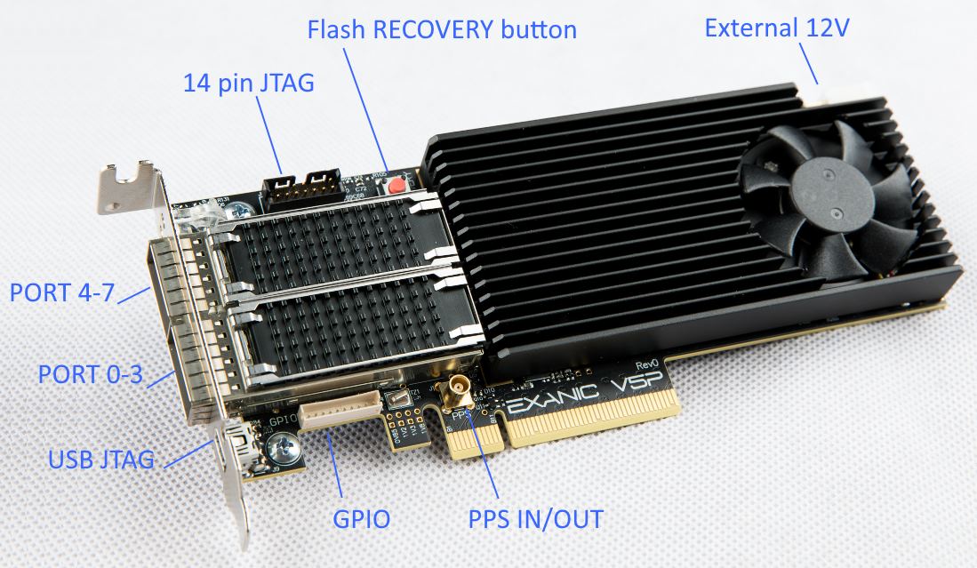
JTAG Access
The SmartNIC+ V5P has several methods for communicating with the FPGA via JTAG.
Xilinx Platform Cable
Users can plug the standard 14 pin JTAG cable from a Xilinx Platform Cable or equivalent JTAG pod into the SmartNIC+ V5P. Note that when this loom is inserted, connectivity from the USB JTAG circuitry to the FPGA is disabled.
USB JTAG
Users can plug a USB cable into a connector on the PCIe bracket of the SmartNIC+ V5P to gain JTAG access to the FPGA. Note that the USB JTAG interface and "14 way" interface cannot be used simultaneously. If a loom is connected between the 14 pin header and a Xilinx pod, the USB JTAG circuitry will be disconnected from the FPGA.
PCI Express
When using the Exablaze Firmware Development Kit, JTAG can be redirected over PCI Express by specifying make JTAG=1 when building a bitstream. Refer to the FDK documentation for more information on this feature. While such a bitstream is loaded, the other access methods cannot be used.
GPIO
A 10 pin connector is available on the SmartNIC+ V5P for user GPIO. GND, 1V8 and 8 bits of GPIO are exposed. Please contact Exablaze for further details on this interface.
PPS
An MCX connector is onboard for PPS in/out time synchronization. Due to size & area restrictions, this connector could not be placed on the PCIe bracket. To use the connector, it is suggested that users run a small loom from the MCX connector to just outside the bracket for connection to a PPS network. Exablaze can supply the loom as well as PCIe brackets that have a small notch in them to allow the loom to pass through easily.
FPGA Development
A Firmware Development Kit is available for the SmartNIC+ V5P to simplify FPGA development, which includes Exablaze's low latency PCS/MAC and DMA engine. Further details on the FDK can be found on our FDK Documentation Site.
For customers using their own IP, the following hardware specific notes may be helpful:
- The full Xilinx part number is XCVU5P-2FLVA2104E (Vivado part name
xcvu5p-flva2104-2-e) - The configuration memory attached is a Micron MT28EW01GABA1LPC-0SIT (NOR BPI x16)
- The PCIe reset net
PERSTN0is inverted on the PCB. When using the Xilinx PCIe core, the System Reset Polarity dropdown will need to be set to ACTIVE HIGH. - PCIe lane reversal is in use (FYI only, the PCIe core will detect and deal with this)
-
161M reference clocks are supplied to the following locations:
- Bank 131 MGTREFCLK0_131, pins V38/V39
- Bank 231 MGTREFCLK0_231, pins W9/W8
- Bank 48 pins AJ32/AK32
- Bank 72 pins K21/J21
-
The following GTY transceiver channels have their polarity inverted on the PCB - the transceiver IP core will need to have
RXPOLARITY/TXPOLARITYset for these:- Bank 131 channel 0 (GTYE4_CHANNEL_X0Y28) TX, pins T42/T43
- Bank 131 channel 3 (GTYE4_CHANNEL_X0Y31) TX, pins K42/K43
- Bank 231 channel 0 (GTYE4_CHANNEL_X1Y28) TX, pins V7/V6
- Bank 231 channel 1 (GTYE4_CHANNEL_X1Y29) RX, pins W4/W3
- Bank 231 channel 3 (GTYE4_CHANNEL_X1Y31) RX, pins U4/U3
This page was last updated on Feb-11-2021.