Cisco Nexus 3550-T FPGA Development
The Cisco Nexus 3550-T Triton
Hardware Overview
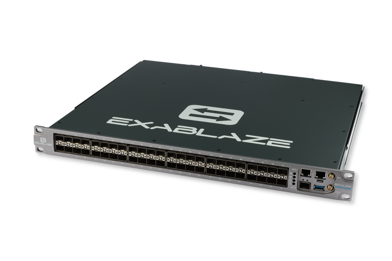
The Cisco Nexus 3550-T Triton platform has a Xilinx Virtex Ultrascale Plus FPGA (XCVU35P-3e), 48 25G capable SFP ports and an Intel Atom CPU. A firmware development kit is available from Cisco, enabling users with FPGA development capability to implement custom FPGA functionality in the XCVU35P-3e FPGA of the Cisco Nexus 3550-T.
Hardware Architecture
A block diagram of the Nexus 3550-T platform is given below.
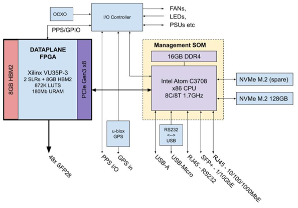
Nexus 3550-T hardware architecture
The FPGA in the Cisco Nexus 3550-T is a Xilinx Virtex UltraScale+ HBM xcvu35p-fsvh2892-3-e.
The X86 processor in the Nexus 3550-T platform is an Intel Atom C3708 SoC, built into a third-party System on Module (SoM). The CPU features 8 cores, running at 1.7Ghz with 16MB of cache. There is 16GB of DDR4 Memory on the SoM, and the system boots from an M.2 NVMe SSD drive, with 128GB of non-volatile storage. There is a spare (unpopulated) M.2 drive bay available.
Connectivity
Transceivers
The XCVU35P-3e FPGA has 56 28Gbps capable transceivers. 48 of them are directly connected the SFP ports. The remaining 8 transceivers are connected to the Intel Atom CPU through a PCI Express (PCIe) interface.
The following diagram shows where the transceivers used for Ethernet and PCIe are located in the FPGA.
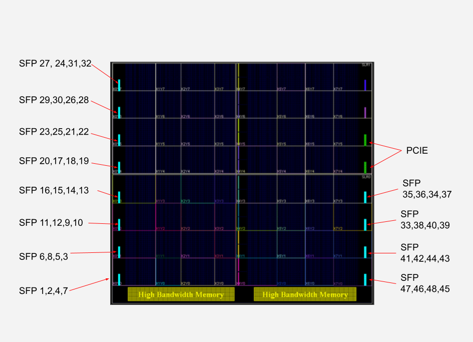
Triton FPGA transceiver placement
PCIe Interface
There is a high speed PCIe interface between the Atom x86 CPU and FPGA module, which is capable of approximately 50Gb/s when configured in Gen3 x8 mode. Please refer to the UltraScale+ Device Integrated Block for PCI Express PG-213.
HBM
There is 8 GB of High-Bandwidth Memory (HBM2) integrated in the FPGA for applications requiring high density and high bandwidth (up to 460GB/s). This can be accessed using the Xilinx Integrated Memory Interface HBM IP. Please refer to the AXI High Bandwidth Memory Controller v1.0 PG-276 for more information.
Configuration
Software Setup
In order to run custom firmware, the Nexus 3550-T must be running the FDK software image instead of ExaOS or NX-OS. This image provides a bare Debian Linux system with platform management daemons and firmware utilities installed.
To install this image from ExaOS, please use the config update file command
with the exablaze-triton-fdk-installer.bin image. Please visit Nexus 3550-T firmware update documentaion for more details.
Warning
This command will replace ExaOS with the FDK software image, which is a minimal Debian Linux system. Any existing configurations will not be applied, such as the management network configuration.
Warning
After initial installation, the FDK software image will only allow log in
on the serial console as root with no password.
For security, please set a root password as soon as possible.
Note
Please refer to the the Debian Reference Manual for instructions on basic system setup tasks, such as setting up the network interface for management.
To remove the FDK software image and revert to ExaOS,
download the exablaze-triton-installer.bin image from here, copy it to the device and
run the following script as root:
# system_update.sh --update exablaze-triton-installer.bin
Warning
The system_update.sh script will erase any existing system image
that is on the device.
Any data on the device (except for data in /mnt/persist)
will not be recoverable!
Software Utilities
Register Read and Write
The FDK software image provides the commands triton-vu35p-reg-read and
triton-vu35p-reg-write.
These two commands can be used to access the register interface.
Refer to the section on Running the reference design for examples of how to use these two commands.
Firmware Update
The program to reflash the FPGA firmware is triton-vu35p-fwupdate.
To reflash and reconfigure the FPGA, use the following command:
# triton-vu35p-fwupdate -r my_project.bit
This will write the bitfile my_project.bit to the flash, then immediately
reconfigure the FPGA using the new bitfile.
Note: During development it is not necessary to transfer bitfiles to the Nexus 3550-T - you can configure the FPGA directly from Xilinx's Vivado Design Suite. Refer to the section on Debugging with Vivado for more information.
Getting Started
Overview
Cisco provides reference designs to get started with FPGA development using the Nexus 3550-T. These examples also include our ultra low latency PCS/MAC. Depending on the configuration, some or all of the 48 transceivers connected to the SFP front panel are instantiated.
The following examples (referred to as targets) come with our development kit, including the requisite source code for each.
- A 'native loopback example' implements a loop-back application, where the received packets on a particular port are looped back out of the same port
- A 'native trigger example' shows how to pre-load Nexus 3550-T with a reply ahead of time, and send it based on a simple mask/pattern match over received frames
Build System
The Nexus 3550-T development kit ships with a build system for various fully
functional target example applications. The build system consists of a Makefile
and a Vivado TCL script (compile.tcl). The Makefile launches Vivado and
instructs it to run the TCL script. All project source files and the Vivado
build process are defined within the TCL script.
The Vivado environment must first be sourced by running the following (change path to suit):
$ source /opt/Xilinx/Vivado/2019.2/settings64.sh
The Makefile expects a TARGET and VARIANT to be provided. The default targets (each of which
are contained within their own directory under the src/ directory) are:
native_loopback_examplenative_trigger_example
Available VARIANTs are full, demo and free.
The development kit is delivered as a tarball. Once this is extracted, the reference design can be built using following command:
$ make TARGET=native_loopback_example VARIANT=full
Users can also create their own targets in a new directory under src/.
The build system will generate a number of files in the outputs/ directory,
including a standard firmware image with a .bit extension that be can be transferred
to the Nexus 3550-T.
Cisco build options
There are several build options that are available for the FDK that Cisco
needs to set at the FDK build time, rather than at the customer's build time.
The file buildlog contains information as to what the build options were set
to at the time the particular FDK was generated by Cisco. The build options
are:
- FDK Type: Specifies whether this FDK is a Full, Free or Demo.
- Number of Ports: Specified the number of ports that are enabled in Nexus 3550-T. The default is 48.
Reference Design Structure
The reference design is intended to be a simple example of how to get started with FPGA development for the Cisco Nexus 3550-T. The reference design instantiates a number of FPGA transceivers and connects each one of them to an Cisco low-latency PCS/MAC.
The top module described in triton_devkit.sv instantiates the triton_devkit_netlist
module which instantiates the Cisco low-latency PCS/MAC module. This top level module provides connections
between the Nexus 3550-T FDK netlist and the user's application. The top module also
instantiates the PCIe and high-speed transceiver IP cores.
An overview of the FDK structure for Nexus 3550-T is shown below.
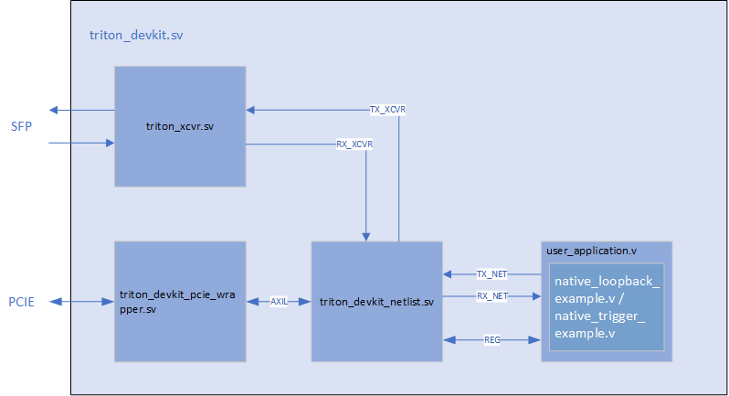
Reference Design Structure
PCIe wrapper
The Xilinx PCIe endpoint IP is instantiated in the module triton_devkit_pcie_wrapper.
The IP is configured to Gen3 x8, and BAR0 is enabled for 16MBytes of memory space. The management processor
accesses FPGA registers via the PCIe bus and register interface.
Triton devkit netlist
This contains the Cisco low-latency PCS/MAC module. It provides full access to all network transmit and receive datapaths, as well as a register space that can be accessed through a management processor by user.
User Application Interfaces
Clocking and miscellaneous
clk_tx_net(1bit) network transmit clock. Alltx_*_netsignals are synchronous toclk_tx_net.clk_rx_net(1bit per port) network receive clock. Allrx_*_netsignals are synchronous toclk_rx_net.clk_mgmt(1bit) a 250 MHz clock generated from clock. register interface is synchronous to this clock.rx_link_up(1bit per port) link_up status for each rx port.
Network Interface
The network-side interface allows the user application to send and receive packets on the network via the Cisco low-latency MAC.
The received data is provided via the following signals, all of which are inputs:
rx_data(32 bits per port) - packet data as received from the wire. The first byte appears at byte 0 (bits 7 to 0).rx_sof(1 bit per port) - asserted on the same cycle as the first data word received from the wire.rx_data[7:0]will contain the first byte of the destination MAC address.rx_early_sof(1 bit per port) - a 'heads up' that the start of the preamble has been received and thatrx_sofwill be asserted in 2-3 cycles.rx_eof(1 bit per port) - asserted on the very last cycle of a received frame. The last bytes seen will include the four byte received CRC.rx_len(2 bits per port) - asserted on the same cycle as the EOF, indicates how many bytes in the final data signal are valid. As an example, if this reads 1, then only the bottom byte of data (bits 7 to 0) is valid. If it reads 0, then there are no more valid bytes in this cycle and the packet effectively finished in the previous cycle.rx_vld(1 bit per port) - asserted to indicate that receive data is valid. Due to the overhead of the 64b/66b encoding used in 10G Ethernet, there may be cycles intra-frame that do not contain valid data. This signal only applies torx_data. You can assume thatrx_sof,rx_early_sofandrx_eofare always valid.rx_err(1 bit per port) - asserted to indicate an abnormal frame termination condition. This can occur when the sender aborts the frame early, or if the link is lost in the middle of a frame. If a frame is terminated withrx_err, there will be norx_eoffor that frame.rx_crc_fail(1 bit per port) - asserted after EOF to indicate that the frame CRC check failed. This assertion normally occurs two cycles after EOF, but this depends on Cisco build options.
A transmit interface is also exposed to the Nexus 3550-T development kit application. The user application can monitor and modify frames that are being transmitted by the host, as well as transmit frames of its own. Ethernet frames transmitted by the user application must start with the first byte of the destination MAC address, and end at the last byte of the payload. Logic within Nexus 3550-T automatically calculates, appends and transmits the CRC. The FPGA application has the following signals which connect through to the Ethernet transmission logic:
tx_data(32 bits per port) - the packet data to be transmitted. The first byte that will be placed on the wire (e.g. the first byte of the destination MAC address) is located at bits 7 to 0.tx_sof(1 bit per port) - to be asserted on the same cycle as the first data word.tx_eof(1 bit per port) - to be asserted on the same cycle as the last data word.tx_len(2 bits per port) - to be set on the same cycle as EOF, indicating the number of bytes of data valid in the last cycle. Likerx_len, this may be 0 to indicate that the frame effectively ended in the previous cycle.tx_ack(1 bit per port) - acknowledge signal provided to the user application. The Nexus 3550-T can be considered to have accepted transmit data from the application for any rising clock edge during which 'ack' is high. If 'ack' is low the same signals should continue to be presented.tx_err(1 bit per port), corrupt the CRC of the current frame. Note that asserting this signal only corrupts the running CRC calculation, it does not terminate the frame. To terminate the current frame with an invalid CRC, asserttx_eofat least one acknowledged cycle after assertingtx_err.tx_eof_no_crc(1 bit per port), ends transmission of the current frame but does not append the frame checksum. Timing of this signal is the same astx_eof. The result of setting bothtx_eofandtx_eof_no_crcin the same cycle is undefined. If this signal is used, it is the responsibility of the user's firmware to append the CRC to the data stream. (Only available for 32-bit native mode 10G operations.)tx_abort_frame(1 bit per port), aborts the current frame without sending an EOF symbol. Timing of this signal is the same astx_eof. If the current 64b/66b block is not full when this signal is asserted, the remainder of the block is filled with zeros. (Only available for 32-bit native mode 10G operations.)tx_ifg_compress(1 bit per port), Forces the transmitted inter-frame gap to the smallest value allowed by the deficit idle count algorithm, i.e. when there is no accumulated deficit. Must be set oneofand held constant until thesofof the next frame is acknowledged. In practice, we expect the user will set it to a constant value if they determine that the downstream network device can handle sustained short IFGs. Use with caution.
All the above signals are synchronous to clk_tx_out.
Note that tx_ack may drop out at any time. Also note that, during the frame,
valid data must be presented on every cycle. There is no way to stall
packet transmission. This is a property of Ethernet, not a limitation of
our implementation.
Note that the width of each of the above signals scales with the number of ports. To select the
set of signals for a given port, use bit slicing. For example, RX data for port 0 will occupy
rx_data[31:0], and RX data for port 1 will occupy rx_data[63:32]. The example designs
show how to perform this bit slicing or indexing for each of the signals on this bus. This note
applies to all of the Ethernet frame interfaces in the FPGA development kit.
Register Interface
A register interface is provided over PCI Express. The FPGA registers can be accessed remotely via a serial server enabled by the Nexus 3550-T management processor.
The 16 megabyte space is divided into 4 banks. Bank 0 is for Cisco internal use.
Bank 1 and bank 2 are available to user via register interface. Bank 3 is reserved.
On this interface, reads and writes happen a full 32 bit word at a time, with
no individual byte enables. All signals in this section are synchronous to clk_250.
The register space byte address assignment is as follows:
| Address | Description |
|---|---|
| 0x000000 - 0x3FFFC | Cisco internal use |
| 0x400000 - 0x7FFFC | User accessible via bar0 register if |
| 0x800000 - 0xBFFFC | User accessible via bar0 register if |
| 0xC00000 - 0xFFFFC | Reserved |
bar0_w_en(1 bit), asserted on the same cycle asbar0_w_addrandbar0_w_datato indicate a register write request from the host.bar0_w_addr(24 bit), the address of the register the host wants to write to. This address increments by 4 for each 32 bit word, i.e. it is a byte offset.bar0_w_data(32 bit), the write data from the host.bar0_r_en(1 bit), a read enable signal asserted withreg_r_addrthat indicates the address is valid.bar0_r_addr(24 bit), the address of the register the host wishes to read. As with the write address, this address increments by 4 for each 32 bit word.bar0_r_data(32 bit) is the data for the register selected byreg_r_addr. Data must be provided whenreg_r_ackis asserted.bar0_r_ack(1 bit) must be asserted in response to a read (whenreg_r_datais valid). The user logic has 16 cycles in which to assertreg_r_ackin response toreg_r_enbefore the read times out.
Example designs
Native loopback example
This reference design implements a loopback datapath, where the frames received from the RX datapath on a particular port are looped back out of the same port. When running at 10G rate, the Frame Check Sequence (FCS, i.e. CRC) in the received frame is removed before retransmitting the data through the same port. The transmitting PCS/MAC generates a new FCS. 3 cycles of buffering is included in the loopback path to prevent TX underrun issues.
Native trigger example
The native trigger example application allows users to pre-load the Nexus 3550-T with a pattern, mask and reply frame. The application performs a match of any incoming frame on port 0 against the pattern and mask, and if a match occurs the application will transmit the reply frame on port 1. This application can be used as a starting point for more advanced custom logic.
Note that this example application is only implemented on the FPGA for port 0 and port 1.
There are a few registers implemented in the user_application.v in the reference
design for test.
| Register Address | R/W | Description |
|---|---|---|
| 0x400000 | R | Application ID , native_loopback_example=10, native_trigger_example=11 |
| 0x400004 | R | Firmware synthesis epoch time |
| 0x400008 | R/W | Read/Write scratch register |
| 0x40000C | R | Receiver Linkup status for port [31:0] |
| 0x400010 | R | Receiver Linkup status for port [47:32] |
Running the reference design
After building the reference design, you will end up with a bitfile in outputs/ which you will need to copy across to the Cisco Nexus 3550-T:
$ sftp admin@mytritonIP
admin@mytritonIP's password:
sftp> put outputs/triton_native_loopback_example_full.bit
Note: For the native trigger example and full build variant, the bitfile will
be triton_native_trigger_example_full.bit.
Once the bitfile is transferred, the FPGA can be reflashed and reconfigured
using the triton-vu35p-fwupdate command:
# triton-vu35p-fwupdate -r triton_native_loopback_example_full.bit
Note: As an alternative to copying the bitfile to the Nexus 3550-T and having the management processor load it onto the FPGA, a remote connection between Vivado on your workstation and the Nexus 3550-T can be established. You can then use Vivado to configure the FPGA with your bitstream, debug using ILA, etc. Refer to Debugging with Vivado for more information.
In order to access the register interface in the reference design,
login to the Nexus 3550-T as root and run the triton-vu35p-register-read command, for example:
# triton-vu35p-reg-read 0x400000
Read register 0x400000 returns the example application ID.
To read/write to the scratch register (address 0x400008), one would do the following:
# triton-vu35p-reg-read 0x400008
0x00400008: 0x00000000 (0)
# triton-vu35p-reg-write 0x400008 0x12345678
0x00400008: wrote 0x12345678 (305419896)
0x00400008: 0x12345678 (305419896)
# triton-vu35p-reg-read 0x400008
0x00400008: 0x12345678 (305419896)
The time/date of synthesis can be read as follows from register 0x400004:
# triton-vu35p-reg-read 0x400004
0x00400004: 0x602af7c9 (1613428681)
# date -d @1613428681
Mon Feb 15 22:38:01 UTC 2021
In order to find the date this version of the FDK was originally built by Cisco, you can read register 0x4:
# triton-vu35p-reg-read 0x4
0x00000004: 0x6029fef5 (1613364981)
# date -d @1613364981
Mon Feb 15 04:56:21 UTC 2021
To test the native loopback example reference design, connect any port from Nexus 3550-T front panel to a packet generator. Then, send packets from a packet generator to Nexus 3550-T. As the transceiver ports are all looped back in the reference design, you should see these same packets received back on the same port.
Testbench and functional model
The Cisco Nexus 3550-T development kit is provided with a full functional model for
all of the individual interfaces. This can be found in the tb/ directory
of the package. The testbench consists of the following files:
test_bench.v, the top level harness that wraps the various modules contained in the functional simulation.control.v, contains various control tasks and generates the timestamp counter.transmit_sim_32bit.v, simulates the Nexus 3550-T Ethernet transmit interface. Will log frames that have been transferred successful and indicate error conditions.frame_sim_32bit.v, simulates the frames received from the wire.test_cases.v, container for user test cases. Users can add their own simulation directives here.start_sim.sh, a shell script that starts the Xilinx simulator in console mode. To start in graphical mode, use the switch-gui.test_bench.prj, a project file for the Xilinx simulator that lists all files that make up the simulation. This file is generated automatically bystart_sim.shwhen a simulation is run.
The example in test_cases.v shows how users can exercise the various elements
of the functional mode, and provides a test case for the example design. Users
can add their own test cases to this file as necessary.
There are two example applications that can be simulated by users,
native_loopback_example and native_trigger_example.
Users can start the example testbench by running:
$ ./start_sim.sh native_trigger_example
This will cause the testbench to be compiled and xsim to start in command line mode. From the xsim prompt, the simulation can be run for 1 microsecond by entering:
% run 1us
For the graphical mode simulation, run:
$ ./start_sim.sh native_trigger_example -gui
Debugging with Vivado
Connecting to the Nexus 3550-T
Xilinx Virtual Cable (XVC) is a TCP/IP-based protocol that acts like a JTAG cable and provides a means to access and debug your FPGA design without using a physical cable. An XVC server can be enabled in the Nexus 3550-T to allow remote connection to the FPGA.
The XVC server can be started using the command xvcserver as follows:
# xvcserver
xvc server listening on port 2540...
The xvcserver command must be run as root.
Note
The xvcserver command does not run the server in the background.
It will be stopped if you press Ctrl-C or if you close the shell.
Since this program provides low level access to the FPGA, we do not recommend running it as a background daemon. It should only be running when it is actively being used for development or debugging.
After the XVC server on the Nexus 3550-T has been enabled, open a Vivado Hardware Manager session as shown:
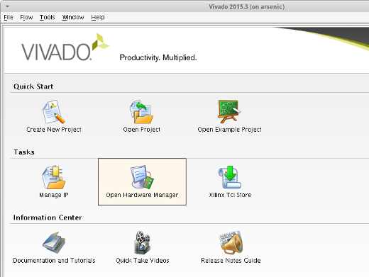
Opening the Hardware Manager
-
Start a Hardware Server session with the following command in the Tcl Console:
connect_hw_server
Ignore the error that may appear if you have no local targets.
-
Connect to the Nexus 3550-T with the following command in the Tcl Console.
open_hw_target -xvc_url 192.168.220.14:2540
The -xvc_url switch tells Vivado the IP address and port to communicate with.
You should now see the FPGA inside the Nexus 3550-T listed, and it can be operated on as normal.
Change history
v1.0.0, 18-Feb-2021
- Initial release.
This page was last updated on May-25-2021.