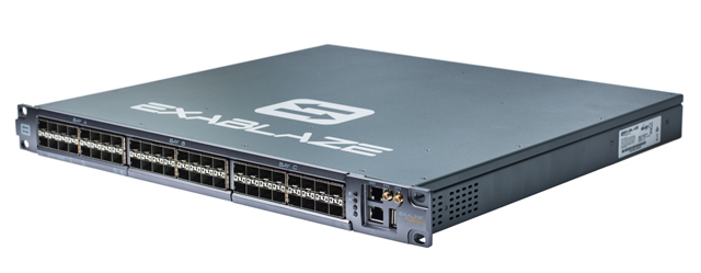
Cisco Nexus 3550-F Fusion FPGA Development
Hardware Overview
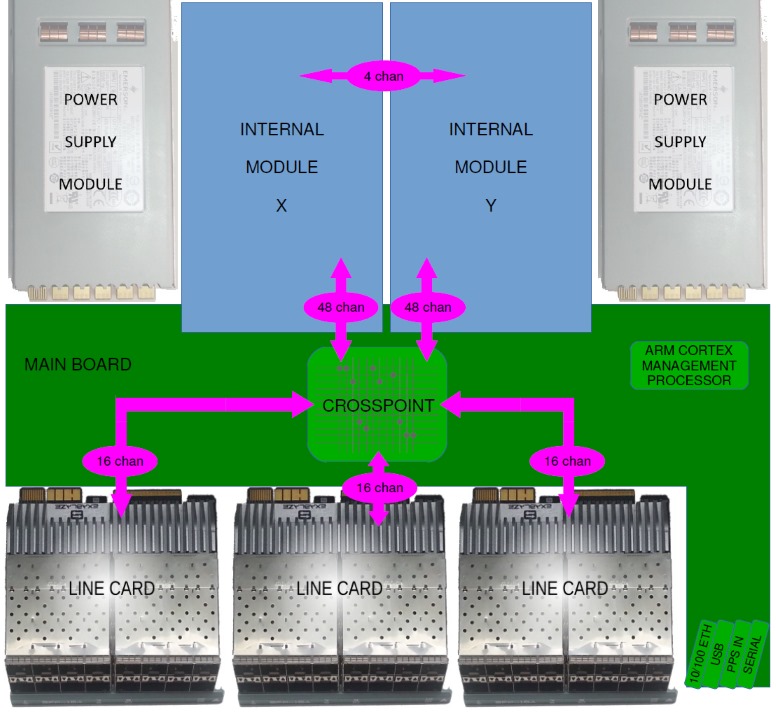
The Cisco Nexus 3550-F Fusion (formerly ExaLINK Fusion) has two internal module bays, one of which is typically populated with an FPGA module running Cisco firmware enabling the creation of mux & switch objects etc. A firmware development kit is available from Cisco which enables users with an in-house FPGA development capability to add custom FPGA functionality into the Nexus 3550-F. A basic version of this development kit is available free of charge from Cisco.
The deployment of user FPGA firmware to the Nexus 3550-F can be either be done in the first FPGA module (i.e. module X), in which case the user's firmware runs instead of the Cisco firmware, or in the second module (i.e. module Y), in which case the system is still able to create mux/switch objects in the first module, and the users firmware runs in the second module. It is also possible to populate both FPGA modules running user firmware. The transceivers in the user's FPGA can be connected directly to front panel ports, or into the other FPGA. If one FPGA is running Cisco firmware, this means that the user's FPGA can be connected to mux/switch objects.
We have reference designs available using this Firmware Dev Kit (FDK), so please contact your Cisco sales representative for further details if you are interested.
Hardware Architecture
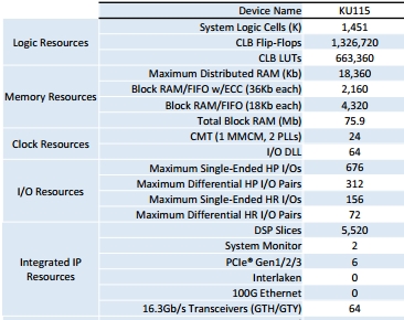
The type of FPGA in the Nexus 3550-F FPGA module is a Xilinx Kintex Ultrascale XCKU115-2FFVD1924C:
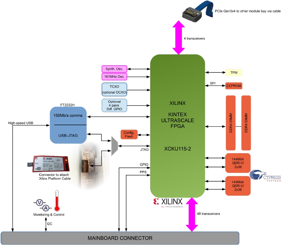
Block Diagram of the Nexus 3550-F FPGA Module
Connectivity
Transceivers
All 52 transceivers are available for use. 48 of these are connected to the layer 1 Crosspoint, where they can then be patched through to front panel ports, or back up into the other internal module. The final 4 transceivers are exposed to a high speed connector that can be directly connected across to the other module, bypassing connection through the Crosspoint.
Note that whilst the GTH transceivers in the Kintex Ultrascale FPGA support operation to 16Gb/s, the rest of the data path from the FPGA to the front panel is limited to 12.5Gb/s.
Sideband Interface
There is a High Speed USB interface between the Mainboard and FPGA module, which is presented to the FPGA as an 8 bit interface along with several handshaking bits. Cisco uses this interface for setting up operating parameters of the FPGA when running mux or switch firmware. When running custom firmware, this communications channel can be exposed out the 10/100 Management Interface port on the front panel. A server is setup on the management processor, and a client can connect via TCP. Any data sent/received through this connection is routed to the FPGA module, allowing users to interact with their design through a non-high speed port for accessing status and configuration parameters. Refer to the serial server section for more information.
Memory
In addition to the ~10MByte of block RAM inside the FPGA, there are a number of additional memories available on the FPGA module.
DDR4 DRAM
There is also a dual DDR4 DIMM interface into the FPGA for applications requiring much higher memory density, accessed using Xilinx's MIG controller.
- In order to fit within the height constraints of the Nexus 3550-F chassis, Very Low Profile (VLP) DIMMs must be used. These have a maximum height of 18.8mm
- Data rates of up to 2133MT/s (PC4-17000) are supported
- Dual-rank ECC (72bit) DIMMs are supported in a x8 configuration
- 16GB VLP DIMMs are currently available from several manufacturers.
Please refer to the Xilinx Ultrascale Memory IP Product Guide PG150 for more information.
EEPROM
A small 1kbit EEPROM is connected to the FPGA via SPI for non-volatile storage of operating parameters etc.
Oscillators and clocking
- All transceivers can either be clocked from a fixed 161MHz oscillator, or a low jitter programmable oscillator for data rates other than 10Gb/s.
- There is a 10MHz TCXO (100ppb stability) fitted as standard for general purpose clocking. This can be upgraded at the time of purchase to a high stability OCXO with a stability of 0.2ppb.
- A PPS signal can be connected to the front panel and routed to both FPGA modules through the Mainboard.
Configuration
Setup
In order to run custom firmware, the FPGA module must first be set to function
custom:
admin@N3550-F> config
admin@N3550-F(config)> module Y function custom
Module Y function set to custom
When a module is set to the function custom, the user has the ability to
power on/off the module:
admin@N3550-F(config)> module Y power on
Module Y powered on
A bitfile is then copied across to the Nexus 3550-F using sftp:
$ sftp admin@N3550-F
admin@N3550-F's password:
sftp> put my_project.bit
Once the bitfile is transferred, the Nexus 3550-F is instructed to associate it with
the particular FPGA module, and then start configuration using the reconfig command:
admin@N3550-F(config)> module Y fpga bitstream my_project.bit
FPGA bitstream file "my_project.bit" selected for module Y
admin@N3550-F(config)> module Y fpga reconfig
FPGA reconfiguration started for module Y
WARNING: Module Y is initializing
These commands form part of the running-config. This can be saved to the startup-config in which case the Nexus 3550-F will setup and reconfigure the FPGA with the specified bitfile upon reboot/power up.
Note: During development it is not necessary to transfer bitfiles to the
Nexus 3550-F - you can configure the FPGA directly from Xilinx's Vivado Design Suite,
however the module must still be set to the custom function. Refer to the
section on Debugging with Vivado for
more information.
Operation
The 48 transceivers in the FPGA which are connected to the Nexus 3550-F layer 1
Crosspoint are referred to as X1, X2,.., X48 and Y1, Y2,..., Y48 depending on the
module. These are ports like any other port
in the system, so can have an alias and description set, be patched to another port,
added to a mux object etc.
Note: Setting the speed of a port in this case just configures the signal recovery circuitry for optimal performance, there is no way the management interface can change the speed at which the FPGA PHY/MAC in the user's application operates at - this is left to the user to handle.
Debugging with Vivado
Connecting to the Nexus 3550-F
Xilinx Virtual Cable (XVC) is a TCP/IP-based protocol that acts like a JTAG cable and provides a means to access and debug your FPGA design without using a physical cable. An XVC server can be enabled in the Nexus 3550-F to allow remote connection to the FPGA module.
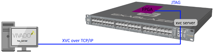
Vivado connecting to the Nexus 3550-F
Once the FPGA module has been configured for custom use, the XVC server is
enabled as follows:
admin@N3550-F> config module y fpga xvc-server port 2542
Hardware server enabled for module Y on TCP port 2542
Warning
Note there is currently no authentication or other security provided on this connection (other than the Access Control List for the whole management interface).
Note
Enabling the XVC server
is not stored as part of the Nexus 3550-F's config, which means it's not listed under
the running-config and that enabling the XVC server must be done each time the
Nexus 3550-F is rebooted. Use the show module command to see the current state.
After the XVC server on the Nexus 3550-F has been enabled, open a Vivado Hardware Manager session as shown:
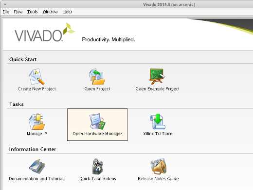
Opening the Hardware Manager
-
Start a Hardware Server session with the following command in the Tcl Console:
connect_hw_server
Ignore the error that may appear if you have no local targets.
-
Connect to the Nexus 3550-F with the following command in the Tcl Console.
open_hw_target -xvc_url 192.168.220.14:2542
The -xvc_url switch tells Vivado the IP address and port to communicate with.
You should now see the xcku115 FPGA inside the Nexus 3550-F listed, and it can now be operated on as normal. For example, right click on SysMon and select Dashboard->New Dashboard to view temperature and voltage status:
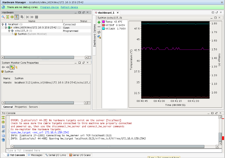
SysMon dashboard showing Nexus 3550-F FPGA status
Refer to http://www.xilinx.com/products/intellectual-property/xvc.html for more information on Xilinx XVC.
Warning
Cisco makes use of bitstream encryption to protect the configuration images shipped with the Nexus 3550-F. The xcku115 EFUSE registers are burnt with encryption key information. The user must NOT attempt to modify any EFUSE settings on the primary Nexus 3550-F FPGA or Cisco firmware can no longer be loaded (unrecoverably) and warranty will be voided. User bitfiles should be generated without any encryption settings.
Configuring the FPGA
In order to configure the FPGA with your custom design, right click on xcku115_0 and select Program Device. A window will appear where you can select the bitfile and click Program. After several seconds, the FPGA will be configured with your bitfile. If your design includes cores such as ILA/Chipscope, MIG or IBERT, these will be displayed under the FPGA along with SysMon.
Once you have finished development of your custom FPGA image, you can transfer the bitfile to the Nexus 3550-F for loading via the management processor, ie without needing to maintain a Vivado session. Refer to the Configuration section for further details.
Example Design
An example design that instantiates 48 transceivers with IBERT cores is available for download here.
First ensure the FPGA module is configured for custom use:
admin@N3550-F> config
admin@N3550-F(config)> module Y function custom
Module Y function set to custom
On the Nexus 3550-F CLI, create several loopbacks by patching internal module ports together, for example:
admin@N3550-F(config)> patch Y1 Y1
Patch created between port "Y1" and port "Y1"
admin@N3550-F(config)> patch Y2 Y2
Patch created between port "Y2" and port "Y2"
admin@N3550-F(config)> patch Y3 Y3
Patch created between port "Y3" and port "Y3"
Enable the XVC server and connect Vivado as described above, then configure the FPGA with the example IBERT bitfile. After the FPGA is configured, you will be asked if you want to auto-detect serial I/O links for the IBERT cores - select Yes.
Depending on how many patches you created above, you will see a number of links detected.
An eye scan can be done on these links by right clicking one and selecting Create Scan,
and clicking OK.
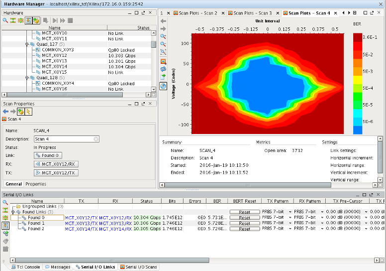
Eyescan of loopback link using Vivado and IBERT
Note these ports can be patched to front panel ports, enabling all 48 ports to run PRBS tests on external equipment. The PRBS pattern can be selected as appropriate, bit errors can be injected etc.
Serial Server
Connection
There is a communications channel between the FPGA and the Nexus 3550-F management processor. When running custom firmware, this channel can be exposed out of the 10/100 Management Interface on the front panel. A server is setup on the management processor, and a client can connect via TCP. Any data sent/received through this connection is routed to the FPGA module, allowing users to interact with their design through a non-high speed port for accessing status and configuration parameters.
To enable this connection the following command is used:
admin@N3550-F> config module Y serial-server port 1055
Serial server enabled for module Y on TCP port 1055
Any port above 1024 can be used for this connection.
Warning
Note there is currently no authentication or other security provided on this connection (other than the Access Control List for the whole management interface).
Beginning with Nexus 3550-F Fusion Software v1.16.0, you can restrict access to the connection
to only the localhost by using the localhost-only option.
To restrict connection access only to the localhost, use the following command:
admin@N3550-F> configure module x serial-server port 9999 localhost-only
Serial server enabled for module X on TCP port 9999 (localhost only)
Framing Protocol
The firmware development kit example uses the HDLC framing protocol to send messages over this interface. HDLC is a serial framing protocol that uses comma and escape codes in order to delimit frame boundaries. The HDLC frame is byte oriented and is structured like so:
| Byte Offset | Contents |
|---|---|
| 0 | Flag byte for SOF (always 0x7E) |
| 1 | Address byte. Bit 0 is always set, bits [7:1] are the peripheral address. Peripheral address is defined below. |
| 2 | Control Byte, always set to 0x03. |
| 3:N+2 | Payload of message, N bytes as specified by the user. |
| N+3 | HDLC Checksum MSB. Unused. |
| N+4 | HDLC Checksum LSB. Unused. |
| N+5 | Flag byte for EOF (always 0x7E). |
Since byte 0x7E is a framing flag, user code should never try to send a byte with this value in any field apart from the SOF/EOF flag fields. Instead, user code should first transmit an escape character, 0x7D, followed by the flag byte with bit 5 flipped (0x5E). If the user code needs to transmit 0x7D, it must follow the same procedure and send 0x7D followed by 0x7D with bit 5 flipped (0x5D).
As an example, for the message payload:
0x50, 0x50, 0x7E, 0x50, 0x7D, 0x50
Would be encoded:
0x50, 0x50, 0x7D, 0x5E, 0x50, 0x7D, 0x5D, 0x50
Example registers
The example design provides an example of using the HDLC stream protocol to expose a 32 bit memory mapped register interface. This registers interface sits at address 0 in the HDLC address space, and allows for read/write messages. The payload structure for this example is as follows:
| Payload offset (DWORD) | Contents |
|---|---|
| 0 | Set to 1 for read request, 0 for write request. |
| 1 | Address of register for read/write request. |
| 2 | Register value (present for writes and read responses). |
As an example, to write to register 1 the value 0x01020304, you would send a HDLC frame that looks like:
0x7e, 0x01, 0x03,       // HDLC Header, address 0
0x00, 0x00, 0x00, 0x00, // Register write
0x00, 0x00, 0x00, 0x01, // Register address 1
0x01, 0x02, 0x03, 0x04, // Register value 0x01020304
0x00, 0x00, 0x7e        // HDLC Footer, zero checksum
For both read and write requests, the FPGA will respond with a HDLC frame that has the same format as a 'write request', however for register read requests, the register value field will contain the value as read from the register
Getting Started
Overview
Cisco provides reference designs to get started with FPGA development using the Nexus 3550-F. These examples also include our ultra low latency PCS/MAC. Depending on the configuration, some or all of the 48 transceivers connected to the crosspoint are instantiated. Users are given the freedom to choose the example application to build from.
The following examples (referred to as targets) come with our development kit, including the requisite source code for each.
- A 'native loopback example' implements a loop-back application, where the received packets on a particular port is looped back out of the same port
- A 'native trigger example' shows how to pre-load Nexus 3550-F with a reply ahead of time, and send it based on a simple mask/pattern match over received frames
A DDR4 memory controller is also included in the design, however it is commented out by default to reduce build time.
Licensing
The Nexus 3550-F development kit can ship as a time limited evaluation version, which is fully functional for up to two hours. After this, features of the evaluation version will progressively shut down and stop working. After this time the host can be rebooted/power cycled to reset the two hour timer. Should you wish to purchase a full license and have this time limitation removed, contact your reseller or your Cisco sales representative to discuss licensing options.
Cisco provides a license file which Xilinx Vivado will require in order to synthesize the "full" version of the development kit. Note that this is not required or provided for "evaluation" FDKs.
This file, exablaze_fdk.lic, is included at the root of the tarball you will have received.
This can be installed either locally or on a license server.
For local installation, the license file can be placed in your ~/.Xilinx/ directory.
You may also need to update your ~/.flexlmrc file to ensure that it has the ~/.Xilinx/
directory in the license search path, it should contain a line similar to:
XILINXD_LICENSE_FILE=/home/username/.Xilinx
For installation on a license server, the license file should be added as a parameter when starting the FlexLM License Server, for example:
lmgrd -c exablaze_fdk.lic:Xilinx_floating_myhost_eth0.lic
If Vivado is unable to locate the license, an error will be generated similar to this:
...
...
Finished Parsing EDIF File [./src/fusion_devkit_netlist.edif]
INFO: [Netlist 29-17] Analyzing 588 Unisim elements for replacement
INFO: [Netlist 29-28] Unisim Transformation completed in 0 CPU seconds
ERROR: [Netlist 29-57] Netlist/bitstream writing will not be allowed because of missing license for netlist cell 'fusion_devkit_netlist', instantiated as 'fusion_devkit_netlist_inst'.
Please refer to the Xilinx documentation and this FAQ for further details.
The Nexus 3550-F FDK can also ship with a 100M & 1G PCS/MAC along with the already included 10G PCS/MAC. All the supplied example applications will work for the 100M & 1G PCS/MAC without any modifications, as long as all the associated ports are configured with equal line rates. The examples may not work as intended when a different line rate is used on downstream and upstream ports as there is no buffering added. Note that the inclusion of 100M & 1G PCS/MAC in the FDK will introduce an additional pipeline stage for 10G in order to meet the timing requirements. This will increase the overall latency of the 10G TX path by one clock cycle.
Software Installation
Prior to using the development kit, customers must install Xilinx Vivado 2015.4 or later, which can be downloaded from the Xilinx website. A synthesis license is required for the FPGA device used in the Nexus 3550-F (XCKU115-2FFVD1924C). A free 30 day “webpack” license is available from Xilinx.
Warning
Cisco has observed instances where incorrect logic is synthesized using Vivado 2016.1 and 2016.2 so use of these versions is not recommended.
Build System
The Nexus 3550-F development kit ships with a build system for various fully
functional target example applications. The build system consists of a Makefile
and a Vivado TCL script (compile.tcl). The Makefile launches Vivado and
instructs it to run the TCL script. All project source files and the Vivado
build process are defined within the TCL script.
The Vivado environment must first be sourced by running the following (change path to suit):
$ source /opt/Xilinx/Vivado/2017.4/settings64.sh
The Makefile expects a TARGET to be provided. The default targets (each of which
are contained within their own directory under the src/ directory) are:
native_loopback_examplenative_trigger_example
The development kit is delivered as a tarball. Once this is extracted, the reference design can be built using following command:
$ make TARGET=native_loopback_example
Users can also create their own targets in a new directory under src/.
The build system will generate a number of files in the outputs/ directory,
including a standard firmware image with a .bit extension that be can be transferred
to the Nexus 3550-F.
Cisco build options
There are several build options that are available for the FDK that Cisco
needs to set at the FDK build time, rather than at the customer's build time.
The file buildlog contains information as to what the build options were set
to at the time the particular FDK was generated by Cisco. The build options
are:
- FDK Type: Specifies whether this FDK is a Full or Demo.
- Number of Ports: Specified the number of ports that are enabled in Nexus 3550-F. The minimum value is 8 and the maximum is 48.
- Extra RX Reg: Specifies whether an additional register stage is added to the internal MAC RX path. This does not impact the user interface/timing diagrams. If this additional register is not included, the MAC latency will improve by 3.1ns, however it will make timing closure more difficult.
- Extra CRC Reg: Specifies whether an additional register stage is added to CRC
RX path. This improves timing closure, but delays the assertion of the
crc_failflag. If this register is added,crc_flagis valid 2 cycles aftereof, otherwise it's valid on the cycle aftereof. - Support for 100M & 1G: Specifies whether 100M and 1G PCS/MAC is included in the FDK. This will also introduce an additional register stage for the 10G PCS/MAC TX path in order to achieve timing closure.
Reference Design Structure
The reference design is intended to be a simple example of how to get started with FPGA development for the Nexus 3550-F. The reference design instantiates a number of FPGA transceivers and connects each one of them to an Cisco low-latency PCS/MAC.
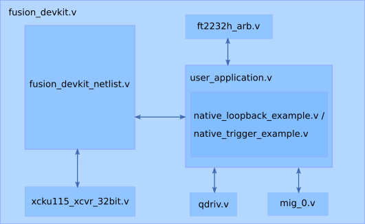
The top module described in fusion_devkit.v instantiates the fusion_devkit_netlist
module which instantiates the transceivers. This top level module provides connections
between the Nexus 3550-F FDK netlist and the user's application. The top module also
instantiates the DDR MIGs.
An overview of the FDK structure for Nexus 3550-F is shown below.
Native loopback example
This reference design implements a native loopback, where the frames received from the RX datapath on a particular port is looped back out of the same port. When run at 10G rate, the Frame Check Sequence (FCS) or the CRC bytes in the received frame is removed before retransmitting the data through the same port. Also, 3 cycles of buffering is included in the loopback path to prevent TX underrun issues.
Native trigger example
The native trigger example application allows users to pre-load the Nexus 3550-F with a pattern, mask and reply frame. The application performs a match on port 0 of any incoming frame against the pattern and mask, and if a match occurs the application will transmit the reply frame on port 1. This application can be used as a starting point for more advanced custom logic.
Note that this example application is only implemented on the FPGA for port 0 and port 1, and all other ports operate as normal network interfaces.
Network Interface
The FPGA transceivers are instantiated in the module xcku115_xcvr_32bit.
The transceivers are connected to the low latency PCS/MAC IP from Cisco,
instantiated within the FDK netlist module. Raw PCS data is then transferred
between the transceivers and the PCS/MAC.
The network-side interface allows the user application to send and receive packets
on the network via the Cisco low-latency MAC. Note that the interface signals
rx_early_sof, tx_eof_no_crc, and tx_abort_frame are only present
in the 10G PCS/MAC and not available for the 100M & 1G PCS/MAC.
The received data is provided via the following signals, all of which are inputs:
rx_data(32 bits per port) - packet data as received from the wire. The first byte appears at byte 0 (bits 7 to 0).rx_sof(1 bit per port) - asserted on the same cycle as the first data word received from the wire.rx_data[7:0]will contain the first byte of the destination MAC address.rx_early_sof(1 bit per port) - a 'heads up' that the start of the preamble has been received and thatrx_sofwill be asserted in 2-3 cycles.rx_eof(1 bit per port) - asserted on the very last cycle of a received frame. The last bytes seen will include the four byte received CRC.rx_len(2 bits per port) - asserted on the same cycle as the EOF, indicates how many bytes in the final data signal are valid. As an example, if this reads 1, then only the bottom byte of data (bits 7 to 0) is valid. If it reads 0, then there are no more valid bytes in this cycle and the packet effectively finished in the previous cycle.rx_vld(1 bit per port) - asserted to indicate that receive data is valid. Due to the overhead of the 64b/66b encoding used in 10G Ethernet, there may be cycles intra-frame that do not contain valid data. This signal only applies torx_data. You can assume thatrx_sof,rx_early_sofandrx_eofare always valid.rx_err(1 bit per port) - asserted to indicate an abnormal frame termination condition. This can occur when the sender aborts the frame early, or if the link is lost in the middle of a frame. If a frame is terminated withrx_err, there will be norx_eoffor that frame.rx_crc_fail(1 bit per port) - asserted after EOF to indicate that the frame CRC check failed. This assertion normally occurs two cycles after EOF, but this depends on Cisco build options.rx_timestamp(32 bit per port) - a counter that serves as the timestamp for the first byte of the received frame with 3.1ns of resolution.
All the above signals, except rx_timestamp, is synchronous to clk_rx.
The rx_timestamp data is synchronous to clk_time.
A transmit interface is also exposed to the Nexus 3550-F development kit application. The user application can monitor and modify frames that are being transmitted by the host, as well as transmit frames of its own. Ethernet frames transmitted by the user application must start with the first byte of the destination MAC address, and end at the last byte of the payload. Logic within Nexus 3550-F automatically calculates, appends and transmits the CRC. The FPGA application has the following signals which connect through to the Ethernet transmission logic:
tx_data(32 bits per port) - the packet data to be transmitted. The first byte that will be placed on the wire (e.g. the first byte of the destination MAC address) is located at bits 7 to 0.tx_sof(1 bit per port) - to be asserted on the same cycle as the first data word.tx_eof(1 bit per port) - to be asserted on the same cycle as the last data word.tx_len(2 bits per port) - to be set on the same cycle as EOF, indicating the number of bytes of data valid in the last cycle. Likerx_len, this may be 0 to indicate that the frame effectively ended in the previous cycle.tx_ack(1 bit per port) - acknowledge signal provided to the user application. The Nexus 3550-F can be considered to have accepted transmit data from the application for any rising clock edge during which 'ack' is high. If 'ack' is low the same signals should continue to be presented.tx_err(1 bit per port), corrupt the CRC of the current frame. Note that asserting this signal only corrupts the running CRC calculation, it does not terminate the frame. To terminate the current frame with an invalid CRC, asserttx_eofat least one acknowledged cycle after assertingtx_err.tx_eof_no_crc(1 bit per port), ends transmission of the current frame but does not append the frame checksum. Timing of this signal is the same astx_eof. The result of setting bothtx_eofandtx_eof_no_crcin the same cycle is undefined. If this signal is used, it is the responsibility of the user's firmware to append the CRC to the data stream. (Only available for 32-bit native mode 10G operations.)tx_abort_frame(1 bit per port), aborts the current frame without sending an EOF symbol. Timing of this signal is the same astx_eof. If the current 64b/66b block is not full when this signal is asserted, the remainder of the block is filled with zeros. (Only available for 32-bit native mode 10G operations.)tx_ifg_compress(1 bit per port), Forces the transmitted interframe gap to the smallest value allowed by the deficit idle count algorithm, i.e. when there is no accumulated deficit. Must be set oneofand held constant until thesofof the next frame is acknowledged. In practice, we expect the user will set it to a constant value if they determine that the downstream network device can handle sustained short IFGs. Use with caution.
All the above signals are synchronous to clk_tx.
Note that tx_ack may drop out at any time. Also note that, during the frame,
valid data must be presented on every cycle. There is no way to stall
packet transmission. This is a property of Ethernet, not a limitation of
our implementation.
For the 100M and 1G PCS/MAC, asserting the signals that are not supported by
the interface will not cause any harmful effects. Generally, this will also not
result in any useful operations. However, it may be worth pointing out that
asserting tx_eof_no_crc will have the same effect as that of tx_eof
for 100M and 1G operations.
Note that the width of each of the above signals scales with the number of ports. To select the
set of signals for a given port, use bit slicing. For example, RX data for port 0 will occupy
rx_data[31:0], and RX data for port 1 will occupy rx_data[63:32]. The example designs
show how to perform this bit slicing or indexing for each of the signals on this bus. This note
applies to all of the Ethernet frame interfaces in the FPGA development kit.
DDR4 Interface
A Xilinx DDR4 memory controller is instantiated in fusion_devkit.v (refer mig_0_inst)
however it's commented out to reduce build time for the majority of customers who
may not need this. Commented out line in compile.tcl will also need to be added back
in if the DDR4 MIG is required.
Note that Nexus 3550-Fs do not typically ship with a DDR4 DIMM installed. In order to fit within the height constraints of the Nexus 3550-F chassis, Very Low Profile (VLP) DIMMs must be used, which have a maximum height of 18.8mm.
Please refer to the Xilinx Ultrascale Memory IP Product Guide PG150 for more information, and contact your Cisco sales representative if you wish to purchase validated VLP DDR4 DIMMs.
Management Interface
The management_if module implements a register interface that can be read and
written through software. These registers can be accessed remotely via a
serial server optionally enabled by the Nexus 3550-F
management processor.
Several other registers are provided, including status of the MIG calibration tests,
port link up status, a synthesis timestamp of the design, and scratchpad registers.
A list of available registers and their details are provided in the table below.
Refer to management_if.v for further details.
| Register | Contents | Attribute |
|---|---|---|
| 0 | Scratchpad register 0 | Read/Write |
| 1 | Scratchpad register 1 | Read/write |
| 2 | Link up status (ports 31 down to 0) | Read only |
| 3 | Link up status (ports 47 down to 32) | Read only |
| 4 | Port rate control (ports 15 down to 0) | Read/Write |
| 5 | Port rate control (ports 31 down to 16) | Read/Write |
| 6 | Port rate control (ports 47 down to 32) | Read/Write |
| 7 | 1G Autonegotiation control (ports 31 down to 0) | Read/Write |
| 8 | 1G Autonegotiation control (ports 47 down to 32) | Read/Write |
| 9 | 1G Autonegotiation status (ports 31 down to 0) | Read only |
| 10 | 1G Autonegotiation status (ports 47 down to 32) | Read only |
| 11 | Timer counter value of last PPS edge | Read only |
| 12 | FDK build epoch time (by Exablaze) | Read only |
| 13 | Firmware synthesis epoch time | Read only |
| 14 | DDR4 MIG calibration status | Read only |
Port rate is 2 bits for each port. The configuration will be as below.
| Port rate bit [1] | Port rate bit [0] | Rate |
|---|---|---|
| 0 | 0 | Reserved |
| 0 | 1 | 100M |
| 1 | 0 | 1G |
| 1 | 1 | 10G |
The 1G autonegotiation control is one bit for each port. When set to 1, this will enable autonegotiation for the particular port. The "autonegotiation complete" status for that port will be available on the corresponding bit in the status register.
Be default, the port rate for each port is set to 10G and the autonegotiation control bits are all set to 1.
Running the reference design
In order to run custom firmware, the FPGA module must first be set to function
custom:
admin@N3550-F> config
admin@N3550-F(config)> module Y function custom
Module Y function set to custom
After building the reference design, you will end up with a bitfile in outputs/ which we'll need to copy across to the Nexus 3550-F:
$ sftp admin@myfusionIP
admin@myfusionIP's password:
sftp> put outputs/fusion_native_loopback_example.bit
Note: For the native trigger example, the bitfile will be fusion_native_trigger_example.bit.
Once the bitfile is transferred, the Nexus 3550-F is instructed to associate it with
the particular FPGA module, and then start configuration using the reconfig command:
admin@N3550-F(config)> module Y fpga bitstream fusion_native_loopback_example.bit
FPGA bitstream file "fusion_native_loopback_example.bit" selected for module Y
admin@N3550-F(config)> module Y fpga reconfig
FPGA reconfiguration started for module Y
WARNING: Module Y is initializing
Note: As an alternative to copying the bitfile to the Nexus 3550-F and having the management processor load it onto the FPGA, a remote connection between Vivado on your workstation and the Nexus 3550-F can be established. You can then use Vivado to configure the FPGA with your bitstream, debug using ILA etc. Refer to Debugging with Vivado for more information.
In order to access the register interface in the reference design remotely, the serial server on the Nexus 3550-F must first be configured:
admin@N3550-F> config module Y serial-server port 1234
Serial server enabled for module Y on TCP port 1234
Several python scripts are included that can read and write to registers from a
remote host to the the FPGA running the reference design via the Nexus 3550-F's
management processor. These are located in the sw/ directory.
Note that you can copy these scripts over to a Nexus 3550-F, and after the serial server has been enabled, drop to a bash shell and run the scripts directly on the Nexus 3550-F itself.
To read/write to the scratch register (address 0), one would do the following:
$ sw/fusion_fdk_readreg.py myfusionIP 1234 0
19088743
$ sw/fusion_fdk_writereg.py myfusionIP 1234 0 99
$ sw/fusion_fdk_readreg.py myfusionIP 1234 0
99
The time/date of synthesis can be read as follows from register 13:
$ sw/fusion_fdk_readreg.py myfusionIP 1234 13
1529990284
$ date -d @$( sw/fusion_fdk_readreg.py myfusionIP 1234 13 )
Tue Jun 26 15:18:04 AEST 2018
In order to find the date this version of the FDK was originally built by Cisco, you can read register 12:
$ sw/fusion_fdk_readreg.py myfusionIP 1234 12
1529990122
$ date -d @$( sw/fusion_fdk_readreg.py myfusionIP 1234 12 )
Tue Jun 26 15:15:22 AEST 2018
Now let's connect the front panel port A1 to the FPGA transceiver Y3:
admin@EXALINK_FUSION> config patch A1 Y3
Patch created between port "A1" and port "Y3"
Then, send packets from a remote host into A1. As the transceiver ports are
all looped back in the reference design, you will see these same packets received
back on the host.
Finally, let's try configuring 1G. First, set the line card port speed to 1G as below.
admin@EXALINK_FUSION> config port A1 speed 1000
Port A1 speed set to 1000
Since A1 is connected to Y3, we need to set the bits [5:4] in register 4
to 0b10 (note that these bits correspond to transceiver port 2).
This can be achieved with the help of the python script:
$ sw/fusion_fdk_writereg.py myfusionIP 1234 4 0xFFFFFFEF
This will configure the rate for transceiver port Y3 to 1G. Now you will be able to
send and receive packets on port A1 at 1G rate.
Testbench and functional model
The Nexus 3550-F development kit is provided with a full functional model for
all of the individual interfaces. This can be found in the tb/ directory
of the package. The testbench consists of the following files:
test_bench.v, the top level harness that wraps the various modules contained in the functional simulation.control.v, contains various control tasks and generates the timestamp counter.transmit_sim_32bit.v, simulates the Nexus 3550-F Ethernet transmit interface. Will log frames that have been transferred successful and indicate error conditions.frame_sim_32bit.v, simulates the frames received from the wire.test_cases.v, container for user test cases. Users can add their own simulation directives here.start_sim.sh, a shell script that starts the Xilinx simulator in console mode. To start in graphical mode, use the switch-gui.test_bench.prj, a project file for the Xilinx simulator that lists all files that make up the simulation. This file is generated automatically bystart_sim.shwhen a simulation is run.
The example in test_cases.v shows how users can exercise the various elements
of the functional mode, and provides a test case for the example design. Users
can add their own test cases to this file as necessary.
There are two example applications that can be simulated by the users viz.
native_loopback_example and native_trigger_example.
Users can start the example testbench by running:
$ ./start_sim.sh native_trigger_example
This will cause the testbench to be compiled and xsim to start in command line mode. From the xsim prompt, the simulation can be run for 1 microsecond by entering:
% run 1us
For the graphical mode simulation, run:
$ ./start_sim.sh native_trigger_example -gui
Change history
v2.7.0, 15-Jan-2021
- Support Vivado 2019.1, 2019.2, 2020.1, 2020.2
- Unify licensing system with SmartNIC FDK
v2.2.0, 19-Mar-2019
- Support Vivado 2018.3
- Add dual DDR MIG (commented out by default)
- Add Vivado licensing requirement for "full" FDKs
- Workaround Vivado issue which caused multi-bit signals to be split up in chipscope
v2.1.0, 5-Dec-2018
- Support Vivado 2018.2
- Add support for 32bit 1G PCS/MAC on all ports
- Add support for 100M Ethernet
- 10G PCS: Add the tx_eof_no_crc_net signal to end a frame without appending the frame checksum
- 10G PCS: Add the tx_abort_frame_net signal to abort the current frame without sending an EOF symbol on the wire
- 10G PCS: Improve SOF selection algorithm in MAC to minimise interpacket gap
- Add extra pipeline stage for 10G to meet timing (only when 1G logic is added)
- Make 1G feature selectable during build time (at Cisco)
v2.0.1
- Mismatch in tx_err_net signal length fixed
v2.0.0, 18-Jul-2018
- Upgrade PCS/MAC to 32b width with reduced latency, 10G only currently
- Add DDR/QDR MIGs (commented out by default)
- Selectable number of transceivers to add to design (at Cisco build time)
- Add a second example design - trigger
- Add support for synthesis with Vivado up to 2018.2
- Add test bench for example applications
This page was last updated on Mar-16-2021.